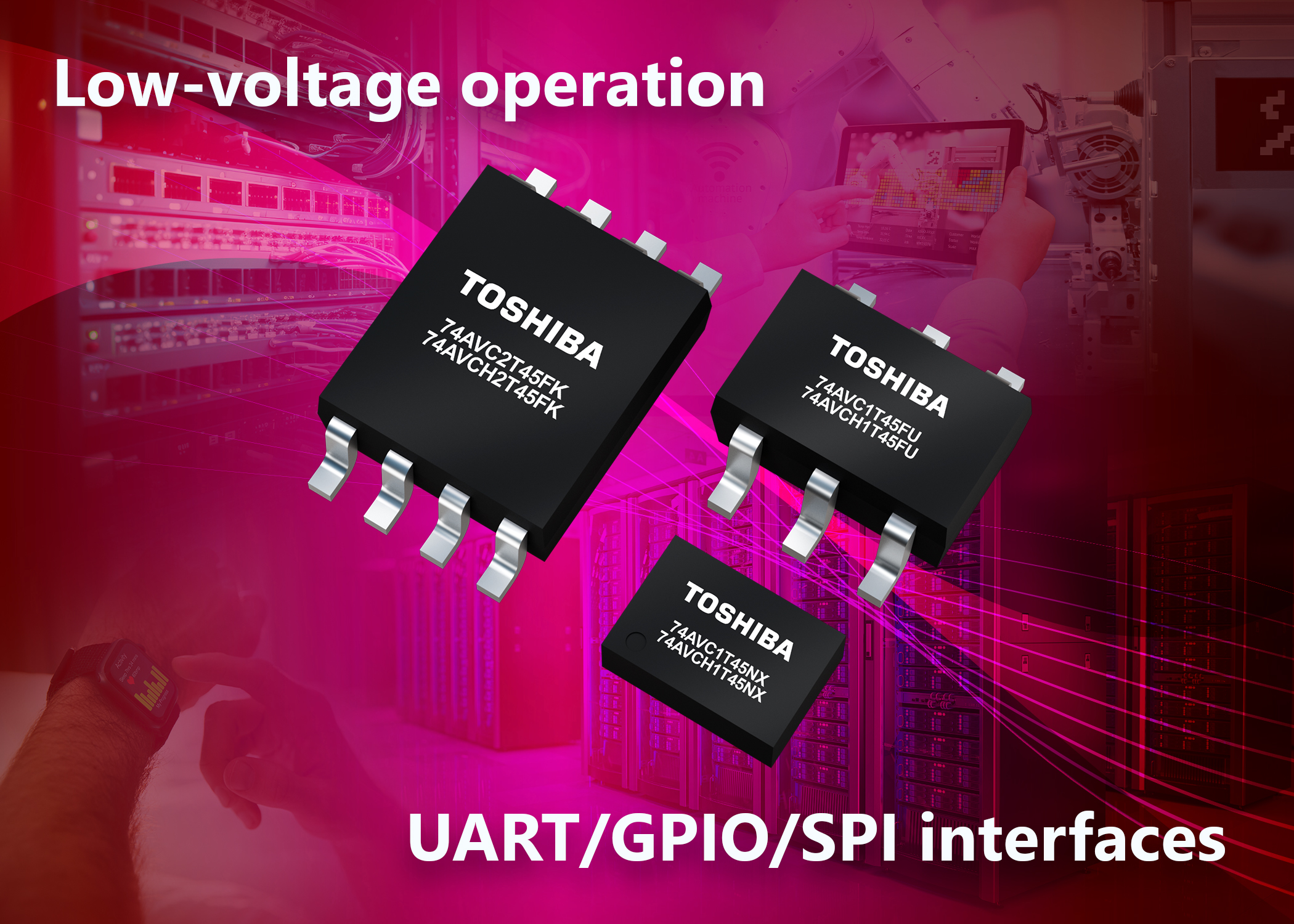
Linear Maximizes Energy Conversion and Launches Hot Swap Devices

Synchronous Buck-Boost DC/DC Converter Offers Low Noise Operation & Extended Run Time from Batteries or Supercapacitors
Linear Technology announces the LTC3113, a synchronous buck-boost converter that delivers 3A of output current from a nominal 3.3V power source, Li-Ion/Polymer battery or up to 1A from dual cell alkaline/NiCad/NiMH batteries. The LTC3113's 1.8V to 5.5V input range and 1.8V to 5.5V output range provides a regulated output from an input voltage above, below or equal to the output. The LTC3113 is also an ideal regulator solution to maximize the energy available from a two supercapacitor stack. The proprietary buck-boost topology incorporated in the LTC3113 delivers a continuous transition through all operating modes, making it ideal for demanding applications that must maintain a constant, low noise output voltage even as the input voltage declines below the output. In many cases, this can add up to 25% more battery run time compared to a buck regulator. The LTC3113's constant switching frequency is user programmable from 300kHz up to 2MHz in order to optimize the balance between efficiency and external component size. The combination of tiny externals and a 4mm x 5mm DFN or TSSOP-20E package provides unprecedented power density, typically required in many high performance applications. The LTC3113 includes two N-channel MOSFETs and two P-channel MOSFETs (RDS(ON) of 29mOhm and 40mOhm, respectively) to deliver efficiencies of up to 96%. User-selectable Burst Mode® operation lowers quiescent current to only 40uA, improving light load efficiency and further extending battery run time. For noise sensitive applications, the Burst Mode operation can be disabled, offering the lowest noise operation. Other features include soft-start, current limiting, thermal shutdown and output disconnect. Summary of Features: LTC3113
- 3A Synchronous Buck-Boost Regulator
- Regulated Output with Input Voltage Above, Below or Equal to the Output Voltage
- 1.8V to 5.5V Input & Output Voltage Range
- Up to 3A Continuous Output Current
- Single Inductor
- Low Noise Buck-Boost Architecture
- Up to 96% Efficiency
- Programmable Frequency from 300kHz to 2MHz
- Selectable Burst Mode® Operation
- Output Disconnect in Shutdown
- Shutdown Current: <1uA
- Internal Soft-Start
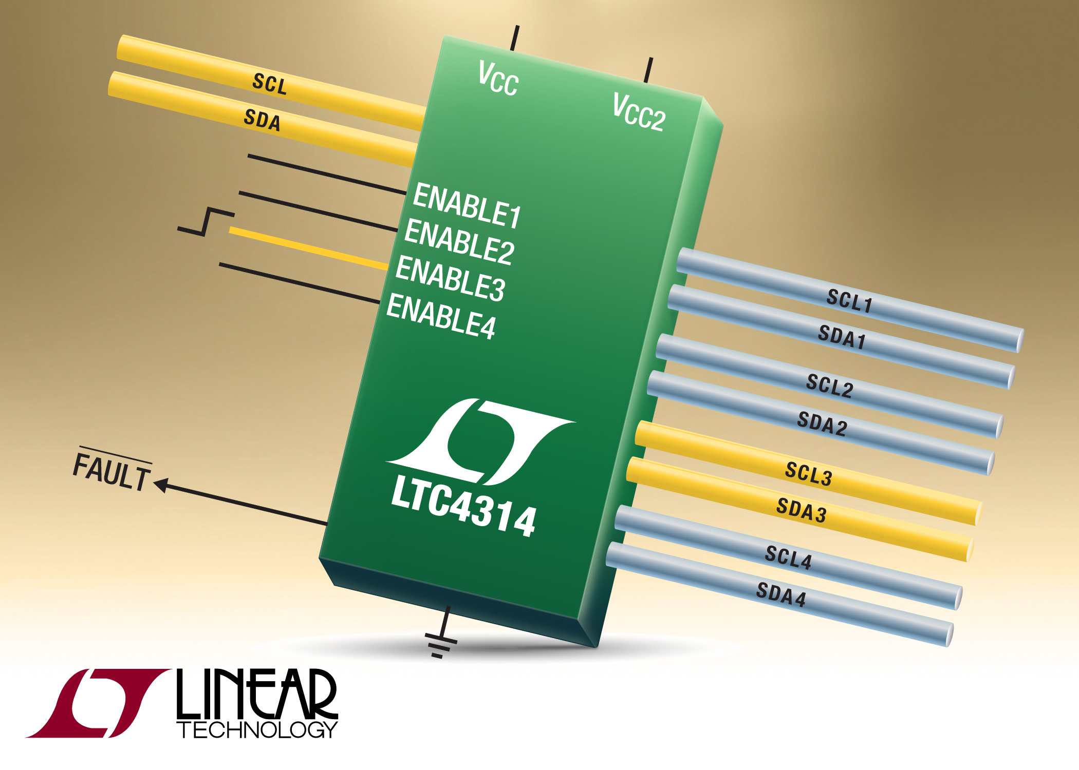
Linear Technology Corporation introduces the LTC4312 and LTC4314 2-wire bus multiplexers, which provide individual enable pins to connect an upstream I2C bus to any combination of downstream busses or cards. The LTC4312 and LTC4314 are pin-selectable multiplexers with bus buffers that reduce component count while promoting ideal I2C signal integrity. The LTC4312 multiplexes two channels, while the LTC4314 multiplexes four channels. These devices allow easy I2C address expansion, providing the ability to address one of multiple identical devices, thus resolving address conflict issues. Bidirectional capacitive buffering allows extension of the I2C bus size well beyond the 400pF I2C bus specification and prevents I2C signal corruption during live board insertion or removal.
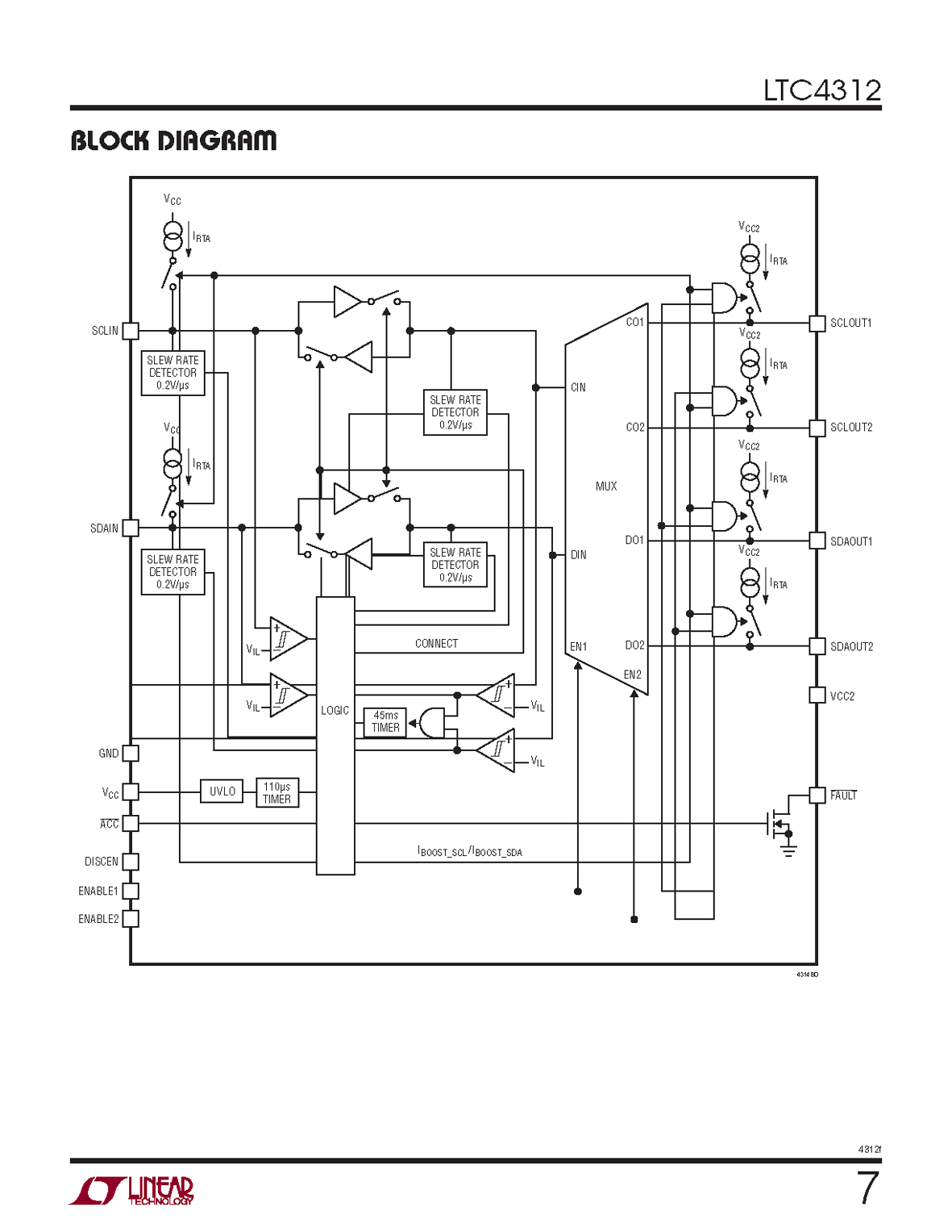
The LTC4312 and LTC4314 are suitable for a wide range of applications, including radial architectures in telecommunications systems such as ATCA, address expansion and level translators. Many I2C and SMBus devices operate at different supply voltage levels, yet must communicate in the same application. The LTC4312 and LTC4314 support level-translation for bus voltages ranging from 1.5V to 5.5V providing the ability to power devices from different supply voltages while maintaining fully bidirectional communications between all devices in the system. Bidirectional buffering keeps backplane and card capacitances isolated, while maintaining low offsets and high noise margins up to 0.3VCC. In addition, built-in rise time accelerators provide strong pull-up currents on SCL and SDA rising edges to meet I2C rise time specifications for heavily loaded busses; the strength of these accelerators can be selected or disabled completely. Safety measures include a stuck bus disconnect and recovery feature to disengage the input from all enabled output channels and issue clocks to the stuck device, a fault output to signal when the host a bus is stuck low, and �4kV HBM ESD protection for increased ruggedness. Summary of Features: LTC4312-14