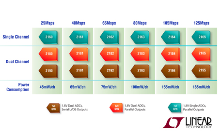
Linear Technology Corporation introduces three families of low power 16-bit, 25Msps to 125Msps analog-to-digital converters (ADCs) that dissipate approximately half the power of competing 16-bit solutions. The LTC2165 and LTC2185 families are single- and two-channel simultaneous sampling parallel ADCs, respectively, offering a choice of full-rate CMOS, or double data rate (DDR) CMOS/LVDS digital outputs with programmable digital output timing, programmable LVDS output current and optional LVDS output termination. The LTC2195 family includes two-channel, simultaneous sampling ADCs with serial LVDS outputs. Each ADC family offers a choice of pin-compatible converters, sampling from 25Msps up to 125Msps - and optimized for the lowest power dissipation at the rated speed. They include such popular features as Linear Technology's digital output randomizer and alternate bit polarity (ABP) mode that minimize digital feedback. These low power 16-bit ADCs enable designers to upgrade performance while maintaining portability in such applications as handheld test and instrumentation, radar/LIDAR, portable medical imaging, PET/SPECT scanners, smart antenna systems and a variety of low-power communication systems. The dual LTC2185/LTC2195 and single LTC2165 consume 185mW/channel at 125Msps and offer signal to noise ratio (SNR) performance of 76.8dB and SFDR of 90dB at baseband. Pin-compatible speed grade options include 25Msps, 40Msps, 65Msps, 80Msps and 105Msps with approximate power dissipation of just 1.5mW/Msps per channel. Further power savings can be achieved by placing the devices in standby (20mW) or shutdown (1mW). Analog full power bandwidth of 550MHz and ultralow jitter of 0.07psRMS allows undersampling of IF frequencies with excellent noise performance. Summary of Features: LTC2165/LTC2185/LTC2195
- 16-bit, 25Msps-125Msps ADCs
- 76.8dB SNR, 90dB SFDR
- Low Power: 185mW/Ch (125Msps)
- Single 1.8V Supply
- Flexible Digital Interfaces:
- LTC2185/LTC2165: CMOS, DDR CMOS or DDR LVDS Outputs
- LTC2195: Serial LVDS
- Selectable Input Ranges: 1VP-P to 2VP-P
- 550MHz Full-Power Bandwidth S/H
- Optional Data Output Randomizer
- Optional Clock Duty Cycle Stabilizer
- Shutdown & Nap Modes
- Serial SPI Port for Configuration
- 48-Pin (7mm x 7mm) QFN Package (LTC2165)
- 64-Pin (9mm x 9mm) QFN Package (LTC2185)
- 52-Pin (7mm x 8mm) QFN Package (LTC2195)