Load switches are increasingly being adopted to play an important part in the management of power and protecting loads in systems large and small
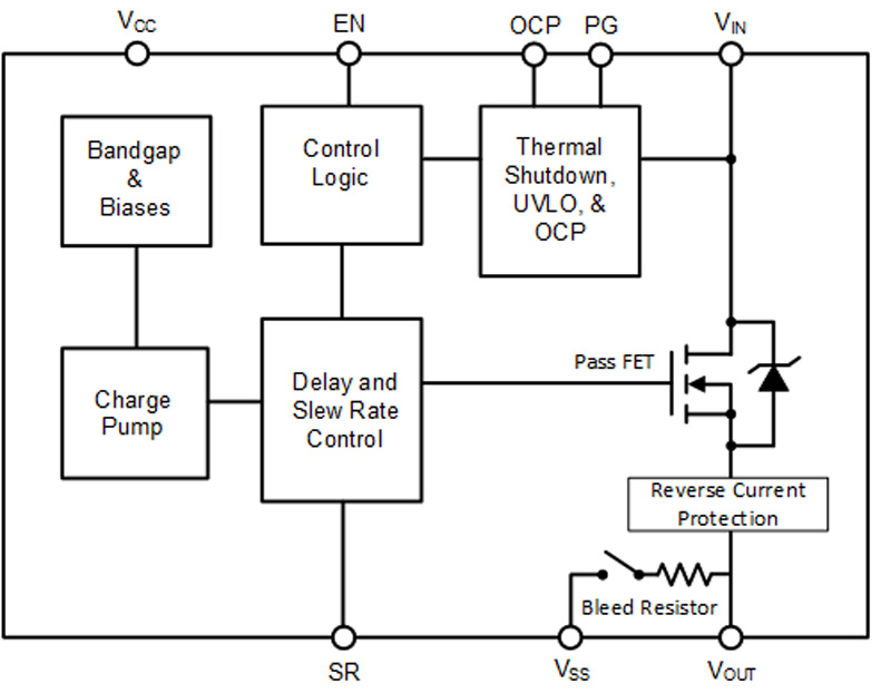
Figure 1: Block diagram of a typical integrated load switch device
Power is the lifeblood of the technology that drives our modern world and, increasingly, we are reliant on high-tech products that assist us in our busy lives both in and away from the workplace. Managing and controlling power is an important topic for high tech, low-power applications. Whether it is developing a sophisticated multi-rail power system for a larger device, or utilizing the very last bit of energy from a battery powered device, power management is high on the agenda of designers.
Load switches play an important part in the management of power and protecting loads in systems large and small. There are several considerations when selecting a load switch for a particular application and, in addition, several new devices with improved performance and capabilities are now available.
Integrated load switch devices
The principal function of any load switch is to connect / disconnect power to a load. This function can easily be achieved with a discrete solution using just a simple pass MOSFET; however, fully integrated load switch devices are generally smaller than discrete solutions, reduce component count, and offer far greater functionality including protection features such as detection and protection for over-temperature, under-voltage, and over–current fault conditions. A further protection that is sometimes included is reverse current protection where any current trying to flow from the load to the source is blocked. This is particularly useful for the latest USB-C standard where power is delivery is used for many applications.
All integrated load switches include a minimum of four pins – VIN, VOUT, GND and EN (Enable) although other pins are often added to support additional functions and provide system outputs for the protection features as shown in Figure 1.
In addition to providing simple on / off control and protection, load switches are also able to control the speed at which the load is turned on through controlling VOUT. By controlling the charging of the FET gate, in-rush current is controlled, as is the rise time of VOUT. This soft startup protects the load from current spikes that can be created by an uncontrolled connection of the load to the power source, especially if the load is not purely resistive.
Some load switches also incorporate a bleed resistor that allows for rapid discharge of any energy stored in the load, eliminating a floating node on the load’s supply pin when the load switch is turned off.
Load switch system uses and configurations
One of the most common applications for load switches is managing separate power domains within a system. This control is particularly useful in battery-powered devices where preventing any unnecessary energy dissipation is critical to obtaining the maximum runtime from the battery.
Load switches can be used to control power to various sections of the system that are segmented into logical domains as shown in Figure 2. In practical use, sections that are only required for a brief amount of time such as sensors or transmit / receive circuitry would only be powered on for the short periods of time they are required to be active.
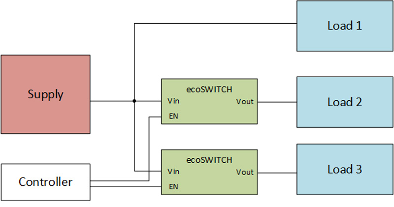
Click image to enlarge
Figure 2: Load switches can manage power delivery across multiple load domains
Additionally, load switches can be used in systems where there are multiple power sources for a single load as shown in Figure 3. Load power can be controlled in such systems to be delivered, for example, from either a main supply or a battery back-up supply.

Click image to enlarge
Figure 3: Power multiplexing allows a single load to benefit from multiple supplies
Complex systems often require multiple power rails and, in many cases, these must be brought up in a certain sequence to facilitate proper operation of the system. For example, it may be necessary for a core processor to be fully booted up before the radio transmitter is enabled to avoid confusing or unintelligible transmissions.
While power up sequencing can be achieved using an external microcontroller to enable the load switches with the correct timing, load switches can also provide sequencing stand-alone with use of a ‘power good’ output as shown in Figure 4. Multiple load switches can be ‘daisy chained’ by linking the Power Good pin of one load switch to the EN pin of the next. If a greater delay between phases is required, a capacitor can be added from the control line to ground to increase the delay.

Click image to enlarge
Figure 4: Load switches can facilitate self-driven power sequencing
Selecting the correct load switch for an application
There are many types of load switches currently available, giving designers a wide choice when selecting a device for a particular application. While at first the choice may seem daunting, by considering six primary parameters it is a relatively simple task to assess the options and find the best device.
Energy efficiency is important and often a key reason for employing a load switch in an application. Designers should pay close attention to the RON resistance of a device under consideration. The lower the switch’s resistance, the lower the voltage drop from VIN to VOUT when operating and, consequently, the lower the power loss and heat dissipated in the load switch.
The device needs to be correctly rated for the application in terms of the maximum permissible load current and the input voltage (VIN) range. While ensuring that the current rating is adequate for the application, care should be taken not to over-specify this rating as larger FETs have higher gate capacitance, requiring more energy to turn on. In addition, a higher rated device is also likely to be larger and more expensive.
The quiescent current (energy used when the load switch is on) should be as low as possible as should any leakage current (current from source to load while the load switch MOSFET is off).
Finally, for certain applications the response speed is critical in terms of the time taken to switch on / off as well as for the timing of any fault protection operation. This response time is affected by the size of the MOSFET with larger devices requiring more charge and consequently being slower to operate. Again, over designing with too large of a FET could lead to poorer transient performance.
ecoSWITCH- A comprehensive range of load switches
The ecoSWITCH series of load management devices from ON Semiconductor provide best-in-class RON resistance currently available to designers. The series comprises of over 20 different offerings and is continuing to grow as ON Semiconductor releases new load switch devices.
The NCP45560 device is just one example of the performance available from the ecoSWITCH series. The device is housed in a space-saving 3 mm x 3 mm DFN12 package yet is capable of switching currents up to 24 A continuously and efficiently with RON values as low as 4.1 mΩ. Ideal for power management and hot swap applications that require a small footprint solution, the NCP45560 incorporates a number of protection features while offering a significant space and cost saving over discrete solutions.
Summary
As power requirements become more complex and the need to operate small, portable battery powered devices as efficiently as possible grows, load switches are becoming more popular, allowing designers to implement highly efficient and sophisticated power schemes even in the smallest of devices.
On Semiconductor