Low Voltage Battery Monitor Floats into High Voltage EVs
System designers need to keep a close eye on both battery and BMS technologies, which can profoundly affect the end-user experience.
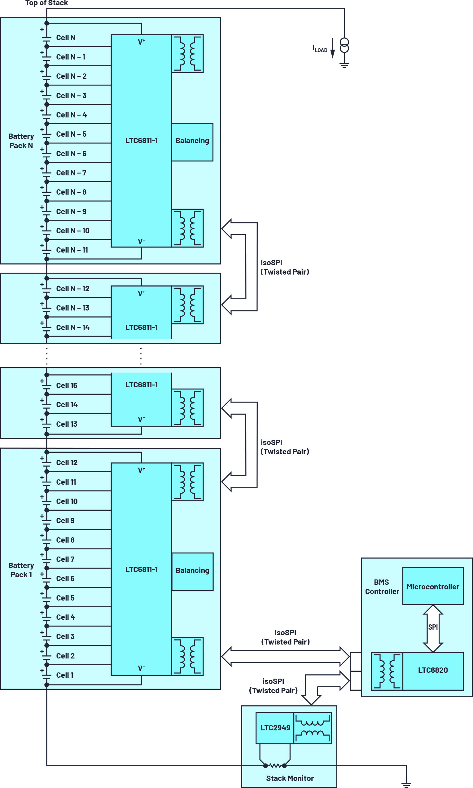
Figure 1. Distributed EV BMS monitoring topology using LTC6811-1s and an LTC2949
For much of the automobile’s history, innovation has focused on improving the fuel burning efficiency of the ICE to clean up emissions. However, the vast majority of recent innovations in ICE automobiles are a direct result of advancements in electronics—improvements in chassis systems, power trains, autonomous and advanced driver assistance systems (ADAS), infotainment, and safety systems. EVs feature many of the same electronic systems as ICE vehicles, plus, of course, the drive train itself. According to Micron Technology, the electronics portion of an EV’s value is as much as 75%, with that portion increasing as advances in semiconductor technology continue to drive down the cost of various electronic modules and subsystems. Even nontraditional automotive players, such as Intel, are looking for a piece of the action.
Not surprisingly, of all the electronic subsystems in an EV, manufacturers and consumers alike focus on the heart of the EV, the battery system. The battery system includes the rechargeable battery itself, lithium-ion (Li-Ion) being the current standard, and the battery management system (BMS), which maximizes battery usage and safety.
BMS Monitoring
A BMS’s primary function is to monitor the state of a battery or, in the case of EVs, a very large pack or stack of batteries. A BMS typically monitors individual cell and pack voltages, currents, temperatures, state of charge (SOC), state of health (SOH), and other related functions, such as coolant flow. In addition to the obvious safety and performance benefits afforded by BMS, accurately monitoring these parameters generally translates to a better driving experience, where drivers are well-informed of real-time battery conditions.
To be effective, the BMS measurement circuits, such as Analog Devices’ LTC2949 pack monitor, must be precise and fast, have high common-mode voltage rejection, consume low power, and securely communicate with other devices. Other EV BMS responsibilities include recovering energy back into the battery stack, balancing cells, protecting the battery stack from dangerous levels of voltage, current, and temperature, and communicating with other subsystems.
Multiple BMS monitoring topologies are used by auto manufacturers to meet their need for accuracy, reliability, ease of manufacture, cost, and power requirements. For example, the distributed topology shown in Figure 1 emphasizes high accuracy with local smarts, high manufacturability with series-connected battery packs, and minimum power consumption and high reliability via low power SPI and isoSPI interfaces for inter-IC communications.
Here, the LTC2949 is used in a low-side current sensing configuration, where the isoSPI communication lines are parallel with the bottom LTC6811-1 battery monitor. For enhanced reliability, a dual communication scheme can be realized by connecting a second isoSPI transceiver to the top of the battery stack and creating a ring topology that can communicate in both directions. Isolated communication with the SPI master controller is implemented via an LTC6820 isoSPI-to-SPI signal converter. Analog Devices’ stackable LTC681x family of multicell battery monitors can be used to measure individual voltages of up to 6, 12, 15, or 18 series-connected battery cells, while a single LTC2949 is used to measure total stack parameters. Together, the LTC681x and LTC2949 form a comprehensive EV BMS monitoring solution—for some, this circuitry might be better known as the BMS’s analog front end (AFE).
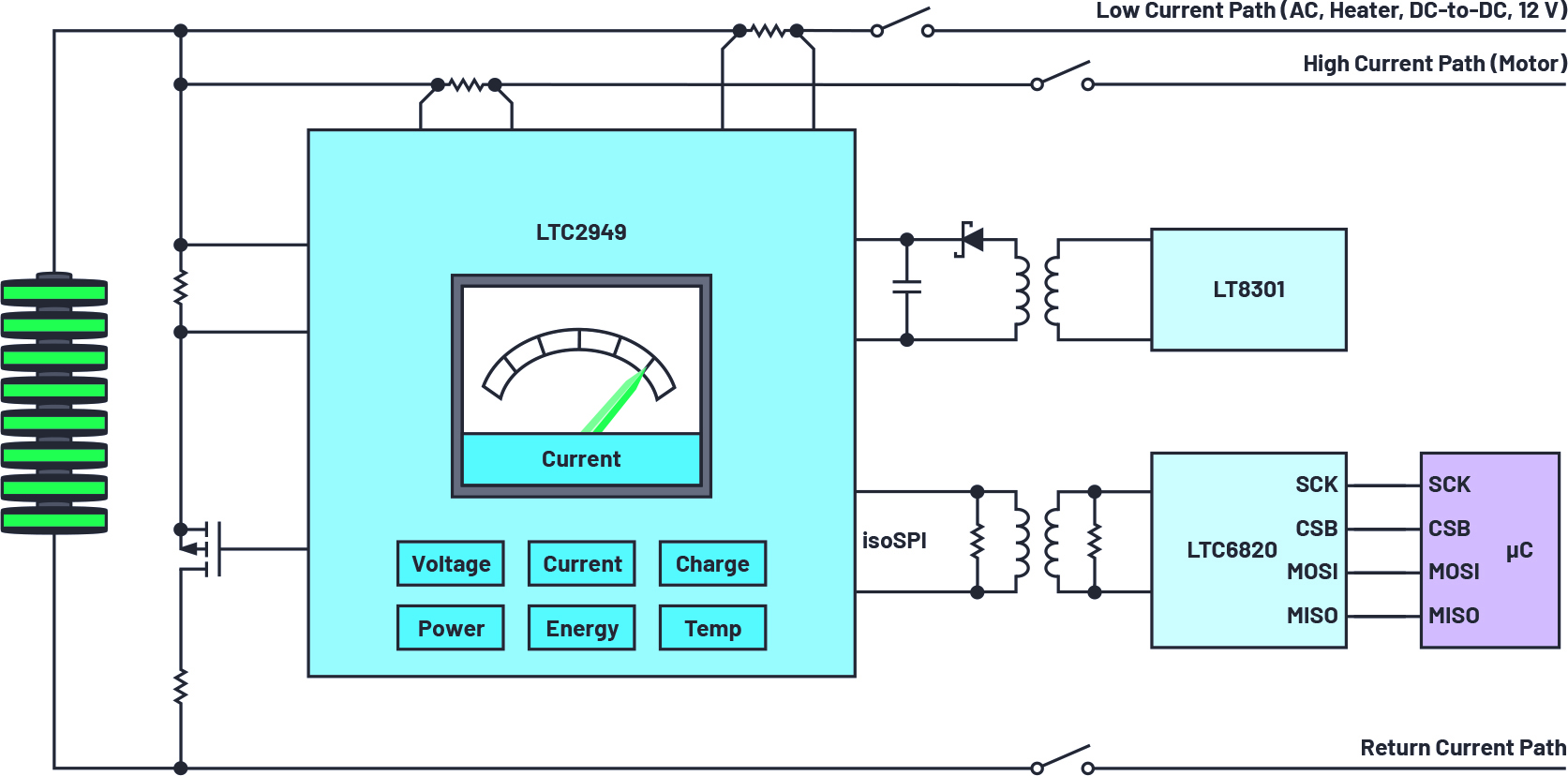
The LTC2949 is a high precision current, voltage, temperature, charge, power, and energy meter that was specifically designed for EVs. By measuring these key parameters, system designers have the essentials to calculate real-time SOC and SOH, as well as other figures of merit, for the entire battery stack. Figure 2 shows a block diagram of the LTC2949 used in a high-side current sensing configuration. Here, the LTC2949 utilizes an adjustable floating topology, enabling it to monitor a very high voltage battery stack, unfettered by its own 14.5 V voltage rating. Power to the LTC2949 is supplied via an LT8301 isolated flyback converter with VCC connected to the positive battery terminal.
Click image to enlarge
Figure 2. Typical hookup of an LTC2949 floating EV battery monitor in high-side current sense configuration. Power for the LTC2949 is supplied via the LT8301 flyback with VCC connected to the positive battery terminal
Ahead with Analog
The LTC2949 has excellent analog performance and can seamlessly integrate into practically any EV BMS. At the core of the LTC2949 are five rail-to-rail, low offset, sigma-delta (Σ-Δ) ADCs to ensure accurate voltage measurements. Of the five ADCs, two 20-bit ADCs are available to measure the voltages across two sense resistors (as shown in Figure 2) and infer the current flow through two separate rails with an impressive 0.3% accuracy; with less than 1 µV of offset, the LTC2949 also offers exceptionally high dynamic range. Similarly, the total battery stack voltage is measured with up to 18 bits and 0.4% accuracy. Two dedicated power ADCs sense the shunt and battery stack voltage inputs, yielding 0.9% accurate power readings. The last 15-bit ADC can be used to measure up to 12 auxiliary voltages—handy for use with external temperature sensors or resistive dividers. Using a built-in mux, the LTC2949 can perform differential rail-to-rail voltage measurements between any pair of the 12 buffered inputs with 0.4% accuracy.
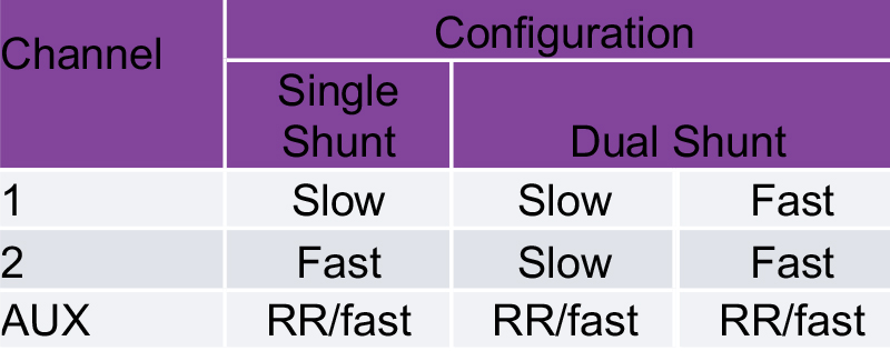
To simplify setup, the LTC2949’s five ADCs form three data acquisition channels. Each channel can be configured for one of two speeds, depending on the application, as shown in Table 1. For example, two channels can be used to monitor a single shunt resistor: one channel for slow (100 ms) high precision current, power, charge, and energy measurements; the other for fast (782 μs) snapshots of current, synchronized to battery stack voltage measurements for impedance tracking or precharge measurements. Alternatively, two different sized shunt resistors monitored by two separate channels (again, as shown in Figure 2) allow users to balance accuracy and power loss for each shunt. Meanwhile, the third auxiliary channel can take either fast measurements of selectable buffered inputs or auto-round-robin (RR) measurements of two configurable inputs, stack voltage, die temperature, supply voltage, and reference voltage.
Click image to enlarge
Table 1. Configuration Options for the LTC2949’s Three Data Acquisition Channels
When any of the LTC2949’s three data acquisition channels are configured for fast mode (782 μs conversion time and 15-bit resolution), the LTC2949 can synchronize its battery stack voltage and current measurements with cell voltage measurements from any LTC681x multicell battery monitor to infer individual cell impedance, age, and SOH. With this information, stack battery life can be assessed, since the weakest cell ultimately determines the SOH of the entire stack.
Since SOH is a point in the life cycle of a battery (or battery stack) and a measure of its condition relative to a fresh battery, it is important to use accurate EV BMS monitors to not only maximize driving range, but to minimize unexpected battery failures. Speaking of battery life, the LTC2949 consumes only 16 mA when turned on and only 8 µA when asleep.
Digital Dominance
The LTC2949’s digital features include an oversampling multiplier and accumulators, producing 18-bit power values, and 48-bit energy and charge values—reporting minimums and maximums, as well as alerts based on user-defined limits. This unburdens the BMS controller and bus from the task of continuously polling the LTC2949 for voltage and current data and the additional task of performing computations based on the results. By taking power samples at the oversample ADC clock rate (predecimation filter) instead of multiplying averaged values, the LTC2949 accurately measures power in the presence of current and voltage variations far beyond its conversion rate, with signals up to 50 kHz.
Because the LTC2949 tracks the minimum and maximum values of current, voltage, power, and temperature data, the bus and host can spend clock cycles on other tasks, instead of continuously polling the LTC2949. In addition to detecting and storing the minimum and maximum values, the LTC2949 can issue an alert if any user-defined thresholds are exceeded—again, releasing the host controller and bus from polling duties. The LTC2949 can also generate an overflow alert after a specified amount of energy or charge has been delivered, or when a preset amount of time has elapsed.
To ensure monitoring accuracy, the LTC2949 provides programmable gain correction factors to compensate for the tolerances of measurement components: two for shunt resistors, a battery voltage divider, and four multiplexed inputs. These correction factors can be stored in external EEPROM to enable a modular approach to factory calibration of battery packs. Moreover, the LTC2949 can linearize temperature readings of up to two external NTC thermistors by solving Steinhart-Hart equations with programmable coefficients; these readings can then be used to automatically temperature-compensate shunt resistor readings. By continuously compensating for both tolerance and temperature effects, not only is monitoring accuracy enhanced, but lower cost external components can be used.
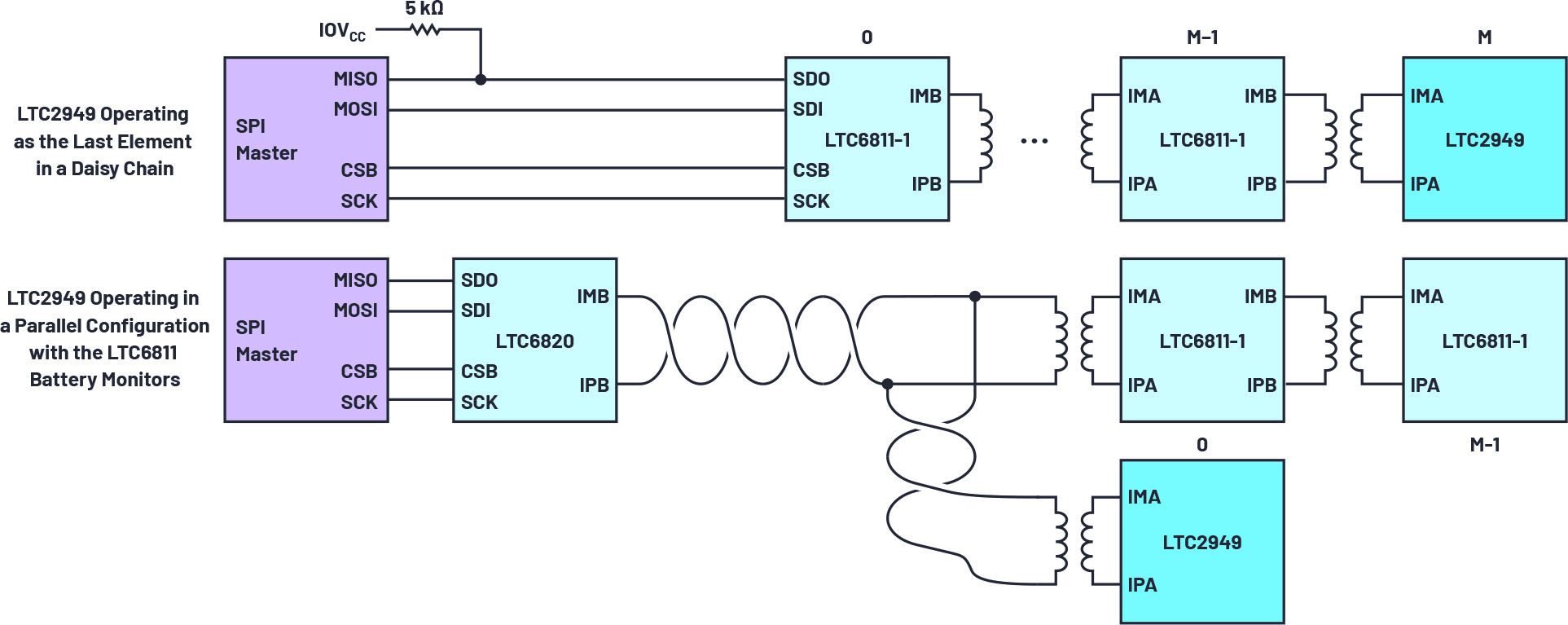
A standard SPI interface is present on the LTC2949 for direct MCU connection. ADI’s proprietary isoSPI interface is also present. isoSPI is a physical layer adaptation of the standard chip-level SPI that unleashes the full potential of cost-effective distributed-pack architectures. Designed for high voltage and high noise systems, isoSPI provides safe and robust information transfer of up to 1 Mbps over up to 100 meters of cable, using only a single twisted pair cable and a simple pulse transformer. isoSPI is also less expensive than other on-board isolation solutions. Figure 3 shows how the LTC2949 leverages isoSPI, along with the LTC6811-1, as the last element in a daisy chain or in an addressable parallel configuration.
Click image to enlarge
Figure 3. LTC2949 isoSPI configurations