Low-Voltage, High-Current Design for Advanced Processing Solutions

Powering industrial, automotive, server, telecom, and datacom applications with advanced system on a chip (SoC), FPGA, and microprocessor solutions
Figure 1: Thermal at 12VIN, 0.6VOUT, 20A load in room temperature
Power solutions for advanced processing require several low voltage supplies, including 1.1V for DDR, 0.8 V for core, and 3.3 V/1.8 V for I/O devices. Because of the high density of semiconductor integration, the microprocessor is more power-hungry and requires more supply current.
There is also a high demand for telemetry using FPGAs or microprocessors that can monitor voltage, current, temperature, and other device parameters. To simplify the design solution, an analog power IC with integrated I2C/PMBus can monitor the key parameters and control telemetry.
As a result, the power solutions must be integrated with I2C/PMBus to enable telemetry readback and regulator programmability while also offering higher current capability, higher efficiency, and excellent electromagnetic interference (EMI) performance. The multiphase parts offering high performance that satisfy those requirements are becoming more popular. In this article, we will introduce some design ideas for a dual-phase step-down regulator that can deliver a total up to 40 A of continuous current from both channels and loads up to 30 A from each channel. It also integrates a digital power system management function allowing for programmability and telemetry with a PMBus/I2C compliant serial interface. Care must be taken to meet the design goals of size, efficiency, loop stability, and transient response.
Why Efficiency Matters
For low-voltage and high-current supplies — for example, an application requires 1V, 30A from a 12V supply — an efficiency of 80% leads to a 7.5 W total loss. Those losses will result in a thermal energy and temperature rise for ICs and inductors. Because the ambient temperature of a data center is usually higher than room temperature, the extra loss will give more temperature rise for ICs and closer to the ICs’ thermal shutdown limit (usually 150°C). This becomes more critical for point-of-load (POL) applications as the DC-to-DC converters are usually very close to the hot microprocessors.
The following sections describe several ways to improve the efficiency for low-voltage, high-current part design.
PCB Trace at the SW Node
In the previous version of a dual-phase part demo board design, inductors from phase 1 and phase 2 face toward each other. The EMI performance is better if the inductors are oriented in this way. The disadvantage of this orientation is that the switching (SW) node will have a relatively long trace, resulting in more PCB trace loss, especially at heavy load conditions because conduction loss is proportional to the square ofthe current value (P = I2R).
Figure 1 shows the thermal image at a 20 A load condition. The switching node is very hot, with almost the same temperature rise as the IC. Proper design can improve the loss caused by the PCB trace.
If the PCB is cut and the Ch1 inductor moved closer to the IC to reduce the SW node trace, based on the copper thickness and length of the PCB trace, the SW node has a DC resistance of 1.01mΩ, with a total loss for a 20A load condition of 0.41W. After reducing the SW trace L = 0.3 cm, the improved loss is 0.17W.
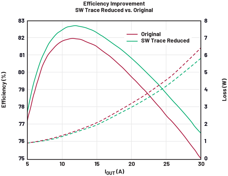
Figure 2 shows the efficiency improvement based on the test results. The loss improvement is 0.22 W for 20 A and 0.53 W for 30 A load conditions.
Click image to enlarge
Figure 2: Efficiency improvement at 12VIN, 0.6VOUT, 1MHz Ch1 FCM VBIAS= 5 V
As load increases, the efficiency difference will be larger, which means the conduction loss (P = I2R) at this PCB trace is dominated. At full load conditions, it can boost efficiency by 1.5%. The inductor cannot be moved this close to the IC, so in Rev2 boards, the inductors are rotated 90° to let them face toward the IC to reduce the SW trace length.
More CIN to Suppress VIN Ringing
In our study, the input capacitors also have a great impact onthe efficiency and stability of low-voltage and high-current applications. Engineers often ignore the importance of the input capacitors’ design and use the previous experience to place the input capacitors. Sometimes, limited by the total PCB solution size, engineers may put fewer input capacitors, leading to instability and more losses.
Click image to enlarge
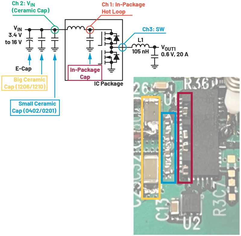
Figure 3: Input capacitors’ block diagram
Figure 3, from left to right, shows an electro-cap for hotplug and suppressing surge currents, the big ceramic caps (usually in 1210 or 1206 size) are for reducing the input current ripples, and the small ceramic caps (in 0402 or 0201 size) are for reducing high frequency ripple. Beyond this, for Silent Switcher 2 technology, a pair of capacitors will be embedded into the package to further reduce the SW high frequency noise and overshoot. The picture on the right side of Figure 3 shows two 1206 ceramic capacitors (in yellow), four 0402 ceramic capacitors outside the package (in blue), and four 0402 in-package capacitors (in red) using the technique of decapsulation. A hole is etched in the package over the die to expose the in-package capacitors over the substrate.
Those input capacitors are probed along with the switching node to observe the behavior of different input capacitor combinations.

Click image to enlarge
Table 1: CIN Combination
However, the trade-off is that the max operating temperature range of the IC has been decreased from 150°C (X8L) to 125°C (X7R). Sometimes, the IC maximum temperature is an important factor to consider because many applications, such as data centers, have an ambient temperature over 70°C. Engineers need to pay attention to those as maximum temperatures may exceed the range if X7R in-package capacitors are chosen.
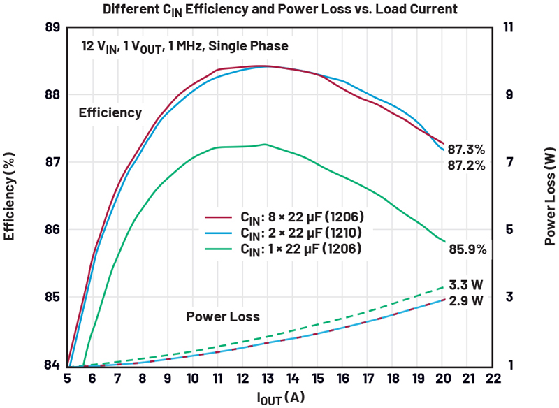
Not only does more CIN improve the stability of switching but it also helps increase efficiency. Figure 8 shows an efficiency improvement of ~1.4% and 0.3 W loss reduction if enough input capacitors are added. The ring and voltage drop at the input side will cause more switching loss. Because 8×1206 size capacitors have similar efficiency to the 2×1210 size capacitors, the optimal CIN selection in this case will be 2×22 µF with 1210 size capacitors.
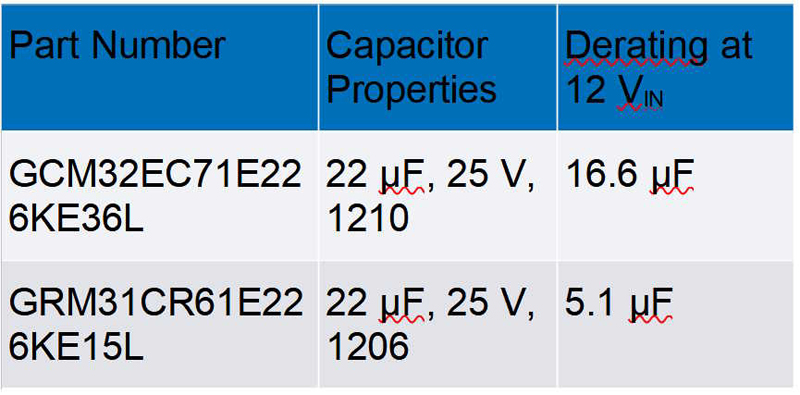
For the input capacitor selection, engineers should also payattention to the DC derating since ceramic capacitors have alarge DC rating range. For example, comparing the DC derating of 1206 and 1210 capacitors at 12 V, the 1206 size will degrade more. In Table 2, two Murata capacitors are listed as an example. Therefore, it’s recommended to use the 1210 size capacitors as the input of low-voltage, high-current power supplies.
If the total input capacitance is small, a large ringing appears at the SW node waveforms during heavy load conditions. This is because when the top switch conducts, most current will be dragged from the input capacitors. Total charge = capacitance times voltage (Q = CV). So, if the capacitance is small, there will be a large voltage drop at CIN. The CIN along with parasitic inductance at the input trace and the IC package will form an LC tank and lead to ringing at the switching node. Large voltage drops will also cause SW distortion and instability where there is a small pulse followed by a large pulse.
The instability of switching can be improved if more input capacitance is added to suppress the ringing. Compared to the small CIN combination, the large CIN combination doubles the values of the total capacitance. The closer CIN is to the top of the switch, the greater the improvement will be. So, it’s better to increase the value of the in-package capacitors. In our case, two 0.1 µF (0402, X8L) is increased to 0.22 µF (0402, X7R)(see Table 1), and the switching becomes stable.
Click image to enlarge
Figure 4: Different CIN efficiency and loss vs. load current
Click image to enlarge
Table 2: Murata Capacitor Comparison
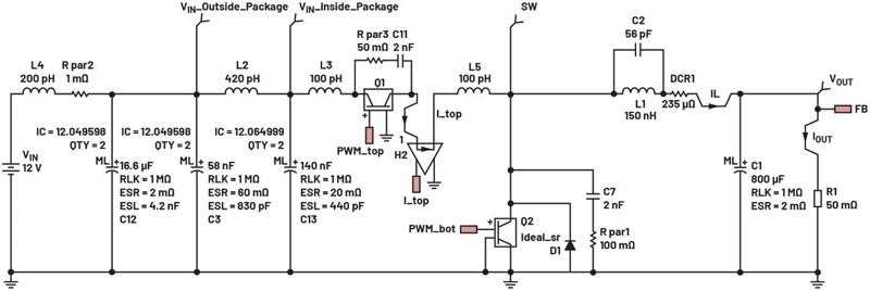
SIMPLIS simulation could be a useful tool to help engineers better design the optimal value of CIN. Figure 5 shows a buck regulator with estimated parasitic inductance along the power trace. The input capacitance has been adjusted according to the DC derating of the ceramic capacitors at 12 V input voltage. Thering will be improved if the input capacitance is doubled from 2× 70 nF to 2× 140 nF.
Click image to enlarge
Figure 5: SIMPLIS simulation schematic