Artificial intelligence enhances 3D FIB-SEM dopant imaging of SiC MOSFETs
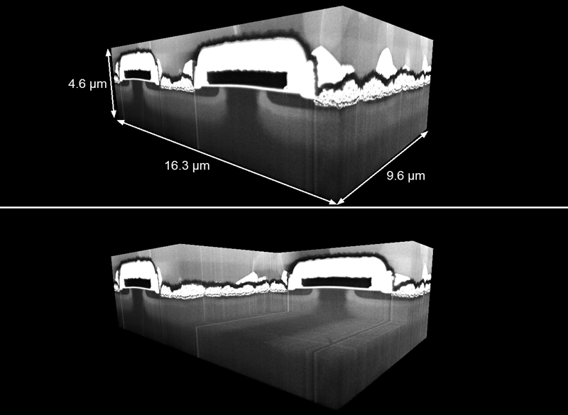
Figure 1. Visualization of a FIB-SEM tomography datasets obtained from a SiC MOSFET samples. The top image shows the full volume, while the bottom one presents the same dataset with a cuboid of approximately one third of the volume cut away....
Silicon carbide (SiC) MOSFETs have become predominantly used in power semiconductors, particularly for automotive applications. To support process development, improve manufacturing yield, and reduce sub-surface failures in finished products, engineers must understand the structure, dopant and junction profiles, and defect morphology of these devices. Imaging a cross-section of such a device with scanning electron microscopy (SEM) can reveal not only its structural details but also its electrically active dopant distributions at high throughput. Such dopant contrast is provided by secondary electron (SE) detection and can be used for examining dopant profiles and for electrical junction localization. At the P-N junction, P regions appear bright in the SE image, while N regions appear dark.
While this type of image contrast is strongest on freshly cleaved samples, cross-sectioning by cleaving has only limited site selectivity. SiC devices are particularly difficult to cleave in a targeted manner. Very high site-specificity can be achieved by focused ion beam (FIB) milling. It produces high-precision, flat cross-sections with excellent surface quality. However, ion implantation and ion-induced amorphization by FIB milling result in an electrically inactive surface damage layer with reduced free carrier concentration. This damage layer causes dopant contrast to decrease with increasing FIB energy. However, in SiC MOSFET power devices strong dopant contrast can be achieved even on cross-sections milled with a gallium (Ga)-FIB at the typically applied high acceleration voltage of 30 kV, if an in-column detector that is particularly sensitive to low-energy SE is used.
3D imaging of dopant regions
The dopant contrast obtained is strong enough to produce not only 2D images but also 3D visual representations of implant regions by FIB-SEM tomography. In this technique, thin layers of material are repeatedly removed from the sample using the FIB, and SEM images are recorded after each removal step to produce an image stack that represents the 3D structure of the sample.
To this end, platinum (Pt) and carbon (C) protective layers are deposited on top of the volume of interest with the Ga-FIB, using gaseous Pt and C precursors. Fiducial lines are cut into the Pt-C sandwich for precise slice thickness and drift control during the data acquisition. A large trench is then FIB milled in front of the volume of interest, followed by an automated iterative slice milling and imaging sequence. Figure 1 shows a resulting dataset that consists of 320 images acquired from a commercially available SiC MOSFET device, using a slice thickness of 30 nm and an imaging pixel size of 20 nm. After data post-processing, the dataset represented a sample volume of 16.3 x 4.6 x 9.6 µm3. The data were acquired in a ZEISS Crossbeam 550 FIB-SEM instrument using the ZEISS Atlas 3D system.
Data visualization and conventional segmentation
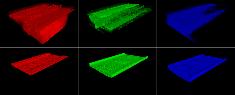
Besides simply scrolling through such an image stack, virtual slices can be extracted from it at any desired position and orientation to inspect structural details (Fig. 2). To inspect individual device components separately in 3D, they need to be separated from the rest of the dataset. This separation process is called segmentation. 3D surface representations of segmented structures are particularly valuable in evaluating dopant distributions, as visualizing their overall shape in 3D provides much more insight into deviations from the intended distributions than simply viewing individual 2D images.
Segmentation by a human operator manually marking the structures of interest in hundreds or thousands of images is prohibitively expensive. Automatic segmentation is required for productive use of the method. However, achieving complete and unambiguous segmentation of different doping levels using conventional pixel grey-value-based segmentation schemes is virtually impossible. In the dataset shown here, three different doping zones can be clearly identified: the dark N+ below either end of the gates, and two different levels of the bright, banana-shaped P+ regions (Figs. 1 and 2). But pixel grey values of the same range as in these zones can also be found in other parts of the dataset that do not represent doping zones. Beyond that, possible image artifacts such as grey value fluctuations originating from local sample charging, shadowing effects due to the adjacent trench walls, or residual vertical FIB milling artifacts (“curtaining”) make the segmentation even more difficult.

Click image to enlarge
Figure 2. XY, YZ and XZ slice triplets taken from the SiC MOSFET tomography dataset. The yellow lines indicate the respective positions of the slices within each row. Note that in the XY column, there is some FIB curtaining visible, extending below the vertical edges of the gate spacers
Conventional segmentation tries to group image pixels according to their grey values by simple thresholding, or by more advanced clustering algorithms that consider statistical properties of the pixel neighborhood. Such segmentation schemes do not provide a clean separation of the different dopant types and levels in SEM images. Figure 3, top row, shows an example. Here, the data were pre-processed by removal of inhomogeneous image background and noise filtering. Then three different pairs of upper and lower gray value thresholds were chosen to select only the pixels belonging to either the N+ or the two P+ zones. The result is that pixels far away from the actual doping zones end up being included in the segmentation, obscuring the actual zones of interest, and rendering 3D visualization useless.
Click image to enlarge
Figure 3. Top row: Attempts to segment N+ (red) and two different levels of P+ doping regions (green, blue) by conventional grey value thresholding. Bottom row: AI-based segmentation result
Artificial intelligence data segmentation
When manually segmenting features in SEM images, human operators do not only use grey values to decide which structural feature a pixel belongs to, but also their expert ability to identify what the feature looks like under the imaging conditions used. A corresponding approach in automatic image segmentation is the use of trainable segmentation. These methods learn domain knowledge by training a segmentation model from pixels labeled by an expert in a small data subset, then applying the model to segment the remainder of the dataset, or other datasets acquired under the same conditions. The model may use an artificial neural network or other machine learning algorithms to decide which pixels belong to which features.
Figure 4 illustrates this process on a single image from the SIC MOSFET dataset. The three different doping zones and the background were annotated by an expert user in only 20 of the 320 images. Adeep learning network model that uses a U-Net with EfficientNet as encoder and Pixelshuffle as decoder was trained on these 20 images with their four annotation classes (ZEISS arivis Cloud, www.apeer.com). The trained model was then used to assign the pixels belonging to each dopant zone and to the background in all 320 images. The result is a clean segmentation of the three dopant zones. Figure 3, bottom row, shows their surface representations. Other than the conventional segmentation, the AI segmentation is free from erroneous components due to unclear pixel allocation and imaging artifacts. It allows us to assess the 3D shapes of the different doping regions and how they relate to the other functional device structures (Fig. 5).

Click image to enlarge
Figure 4. Left: One image from the dataset. Center: Same image with the three different dopant zones (red, green, blue) and background (yellow) annotated by an expert. Right: The predictions of the trained model overlaid to the same image
Click image to enlarge
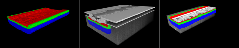
Figure 5. Left: 3D representation of the three AI-segmented doping zones combined. Center: Same visualization overlaid to a 3D representation of the full dataset. Right: The same visualization as in the middle image but cropped to make the inner sample structure visible
Conclusions
3D imaging of SiC MOSFET power device architecture and dopant regions can be performed by FIB-SEM tomography using 30 kV Ga-FIB and an in-column detector sensitive to low-energy SE. However, manual or conventional automatic segmentation of such data to examine the structure of each dopant zone separately and unambiguously is not possible. AI-based segmentation provides a clean separation of the different dopant types and levels. 3D surface representations of dopant zones segmented in this way enable thorough evaluation of implant distributions, as visualizing their overall shape in 3D provides more information about deviations from the intended distributions than simply viewing individual 2D images. This information helps engineers improve yield and reduce failures of SiC power semiconductors.