Meeting PC Power Titanium specifications at light load
A novel digital power factor compensation method provides a higher power factor than ever.
For AC/DC power supplies, there is by nature phase differences and distortion between input currents and voltages due to the existence of holding capacitors and various load features. Here, only the instantaneous product of current and voltage produces power that can actually be used by the appliance, and the power that goes unused reduces the energy potential of the AC line, making it harmful. In addition, the input current that is not in a pure sinusoidal shape also increases line harmonics, EMI (electromagnetic interference), and RFI (radio frequency interference) produced by the power supply, hence affecting other nearby appliances, as well as the power line itself.
Power factor (PF) is defined with the following ratio:
"PF = real power/apparent power"
Here, real power is the average of the product of the line current and voltage over a power line cycle, and apparent power is the product of RMS current and RMS voltage. If the line current is sinusoidal and in phase with the voltage, then PF = 1.
Multiple global regulatory agencies have proposed and enforced standards on power factor and harmonics for different applications. Such agencies include IEC61000-3-2, Energy Star, and so on. For early versions of these standards, only the efficiency and PF at high-load were listed, but the efficiency and PF at zero to low-load have since become important due to the size of modern data centers and industrial/commercial zones. Distortions at low-load can also accumulate to substantial levels.
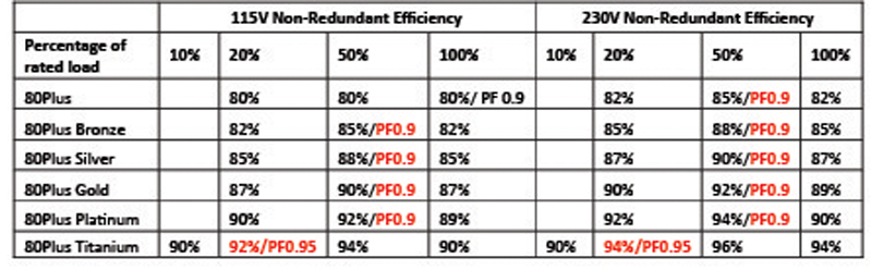
For example, the 80PLUS spec is widely accommodated for computer power supplies and has been added to Energy Star from 2007-2012. The Bronze, Silver, Gold, Platinum specs have been proposed in sequence to manufacturers, and each spec requires higher efficiency and PF than the last. For the Titanium spec, the PF requirement at 20% load is especially challenging for many manufacturers. As of today, out of over 5,300 power supplies that have 80PLUS certification, only 27 of them (0.5%) are Titanium specified (see Figure 1).
Click image to enlarge
Figure 1: 80PLUS Spec
Let’s examine a novel digital PF compensation method. It not only substantially improves PF at light-load, but also benefits full-load conditions at no additional cost. The technology used here not only applies to PC/server power, but also can be adapted for use in gaming consoles, LED street lights, TVs, notebooks, and other battery chargers that are >70W. The complete IC and evaluation board solutions were tested, and the results are shown later in Figure 11.
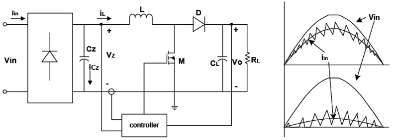
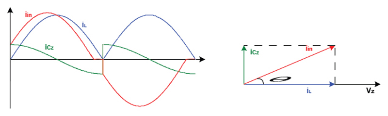
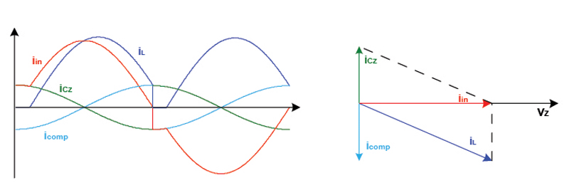
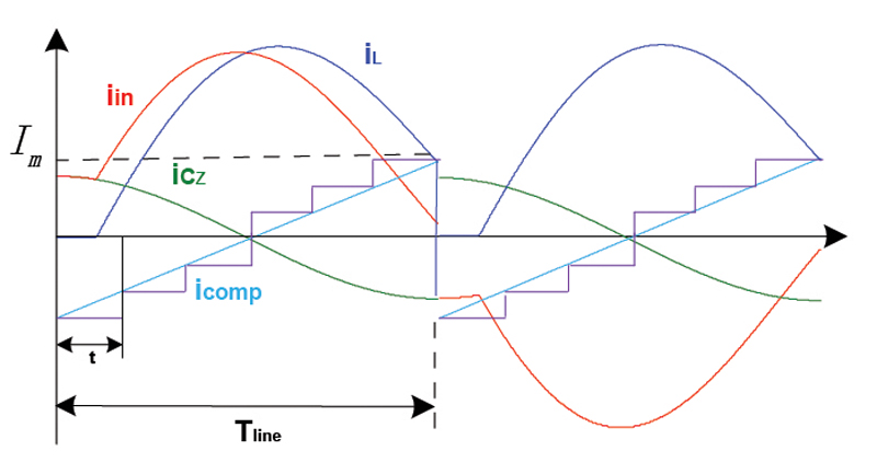
In a power factor correction (PFC) boost converter, there is a small capacitor beyond the input rectifier stage used to supply the high-frequency portion of the inductor current via the shortest path. This capacitor also acts as part of the EMI filter. This capacitor must be chosen at the minimum rated input voltage.2 For all PFC circuits, the control circuit will only shape the inductor current (I_l) to be in phase with the input voltage (V_in). However, as the real input current I_in=I_cz+I_l (where I_cz is the input capacitor current), inevitably there is some current distortion created by the input capacitor (see Figure 2 and Figure 3).
Click image to enlarge
Figure 2: Current Distortions Due to Input Capacitor for Boost Converter
Click image to enlarge
Figure 3: Relationship of the Input Current, Inductor Current, and Input Capacitor Current
The instantaneous input voltage (V_in) can be expressed as:
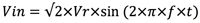
Where Vr is the RMS value of the input voltage, f is the line frequency, and t is the time variable.
The capactitor current (Icz) can be expressed as:
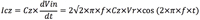
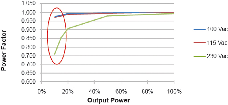
From Equation 2, it is clear that with a higher line voltage (Vin), Icz becomes larger. Since I_l is smaller here compared to low-line at the same load, PF is worse at high-line. At mid-to-peak load, most current will flow through the inductor, and the input capacitor’s current distortion is proportionally smaller, so PF can be >0.9 with a universal input. However, since Ic is not load-dependent at light-load, it becomes relatively high, and PF is more strongly affected. PF drops greatly at high-line and light-load, as shown with the red circle in Figure 4 (from the Onsemi PFC Handbook, page 81). This is where PF fails the Titanium spec for a traditional CCM PFC design. Such behavior is also commonly known in other PFC ICs.3 The actual PF performance may differ from this figure for the actual design, but the trend is always valid.
Click image to enlarge
Figure 4: Traditional PFC
In order to improve PF at low-load and especially at high-line, we need to provide a means to compensate for the capacitor current to the inductor current reference. Instead of the traditional method of matching Il in the same sinusoidal shape as Vin, we match Iin with Vin, which is more ideal for PFC. Since the analog current sensing on the capacitor current requires more components and adds to the complexity, we are introducing a digital compensation method that only uses the existing input voltage signal. This uses the same portion as a traditional analog PFC, but without additional BOM or cost (see Figure 5).
Click image to enlarge
Figure 5: Compensation of the Input Capacitor Current
From Equation 2, we want the compensation current to be the reverse of Icz, rewritten here as:

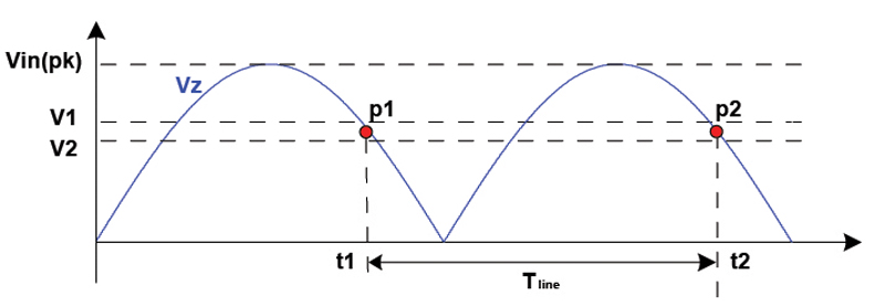
First we need to detect the line frequency (f) from the input voltage sensing network based on a traditional PFC circuit (resistor divider, mostly). We will then be able to detect the line voltage peak (Vin(pk)) per each half-cycle. As Vz falls between V1 and V2 as two sampling points, we leave p1 as a time stamp, and we measure the time interval between two time stamps to decide the line frequency and monitor the line frequency change during operation. This is only realized in digital PFC (see Figure 6).
Click image to enlarge
Figure 6: Detect Line Frequency
Vr is provided by the same input voltage sensing circuit.
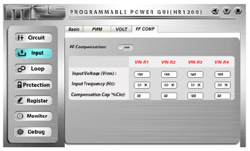
In the digital PFC GUI settings, the value of Cz is fixed for each design and is provided as one of the required inputs to optimize performance (see Figure 7). Users can select the input capacitor value in the actual design first before selecting how much compensation current is desired in proportion to the input capacitor current within four different input voltage ranges (see Figure 8). Note that setting the compensation to >80% will provide >0.95 PF generally, and over-compensation may result in a distorted II.
Click image to enlarge
Figure 7: Digital PFC Configuration Window
Click image to enlarge
Figure 8: Compensating Capacitor Current Setting
The last step is to calculate each cos(2×π×f×t) value during the line cycle. We need to discretize the sinusoidal waveform to be processed in the digital IC. We may use the quasi-sinusoidal or triangular wave approach, as shown in Figure 9 and Figure 10.
Click image to enlarge
Figure 9: Discretize as Quasi-Sinusoidal Waveform
Click image to enlarge
Figure 10: Discretized as Triangular Wave
Although the quasi-sinusoidal method may simulate the waveform better with the same number of samples, it would require some memory size of a complex inverse cosine value table, and would require more calculating power for each time interval. This is not ideal if the line frequency fluctuates. This approach is unfavorable if the digital IC is to be created in the same cost range as a traditional analog IC.
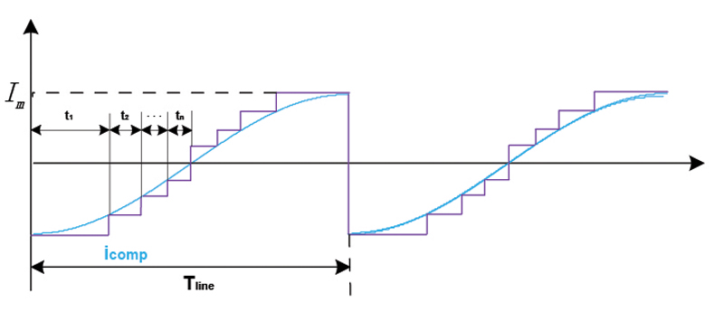
Instead, we have decided to use the triangular approach (see Figure 10). Here, the sampling time interval is kept constant and is updated automatically with line frequency changes, without any additional calculation required.
The amplitude relationship between the fundamental harmonic of a triangular wave and a sine wave is:
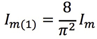
Where I_m is the amplitude of the triangular wave, and I_(m(1)) is the fundamental harmonic amplitude. I_m should be:
The binary code of the compensation current amplitude is:
Where bit_num is the ADC data bit, and V_(adc_ref) is the reference voltage of ADC.
If we divide D_icomp value into N steps in a quarter of a sin wave and make N = D_icomp, then the time interval of each Nth step is:
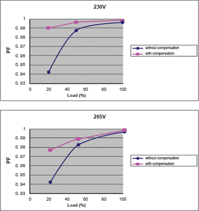
Figure 11 shows the experiment result of the proposed compensation method of the input capacitor current. PF is improved especially at high-line and light-load, so the Titanium spec can be met at no additional cost.
Click image to enlarge
Figure 11: Improved PF at High-Line and Light-Load, with and without Compensation
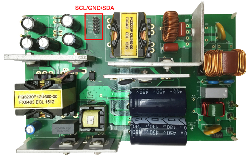
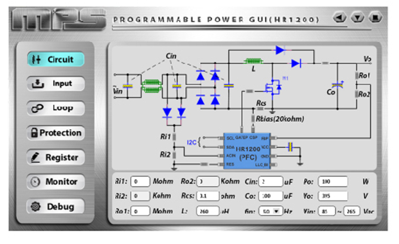
The technology introduced here was first realized in MPS’s HR1200, a digital PFC+LLC combo controller with graphic user interface (GUI). This IC provides customers with state-of-the-art efficiency and PF from no-load to full-load at no extra cost, compared to the traditional analog controller. The HR1200 also provides a GUI for customers to configure multiple functions easily without having to change hardware. Evaluation boards (EVB) and various supporting documents are offered to help customers become familiar with this digital platform (see Figure 12).