Meeting Power Management Enhanced Efficiency, Reliability and Safety Requirements
The SMPS topology used determines the magnetics component solutions within the design
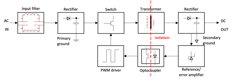
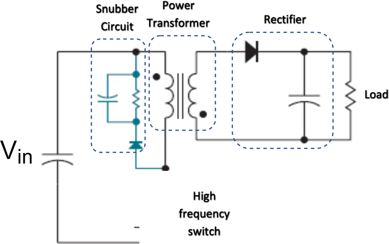
Figure 1. General Block Diagram of a Switch Mode Power Supply (SMPS)
Power conversion, isolation and accurate current measurement along with overvoltage/overcurrent circuit protection are necessary elements in a power supply design. Not only are these component solutions needed to help enhance reliability, but they are also required for regulatory compliance to help increase safety and reduce downtime in these applications. To assist designers, this article outlines the magnetics, resistive devices and protection solutions that are typically required throughout a switch mode power supply (SMPS).
Magnetic Component Considerations
Depending upon the SMPS topology used, designers will need to specify several magnetics component solutions within the design. There are several forms of power conversion in terms of direct current (DC) and alternating current (AC) applications. However, the connotation of “current” in the description is a bit misleading as the functional basis for “DC” and “AC” is a suffix for the type of voltage input to output the SMPS will be used for – DC-DC and AC-DC, for example. In addition, the term “DC” implies a frequency switched DC voltage with respect to the magnetics.
In simple terms, the switched input and output voltages along with resulting changes in current create the construct of a typical SMPS block diagram.
From each block of Figure 1, the use of each magnetics component can be introduced. Depending upon whether the supply is isolated or non-isolated, block sections such as the input filter stage will still represent a magnetic component.
Input Filter Block
The input filter stage prevents electromagnetic interference (EMC/EMI) generated by the SMPS from returning to the power line (i.e., the “grid”). Magnetics components typically used here are a common mode choke (CMC), a differential mode choke (DMC), or a combination of both plus accompanying capacitors to form a filter to block the unwanted noise signal. Both types of components introduce a high impedance at the noise frequency to attenuate the noise from the power line. The difference between the two components is that a CMC rejects common mode currents (noise return to reference ground via parasitic capacitance) flowing through a two-winding magnetics component at the same time. A DMC rejects differential mode currents flowing on both power lines in equal and opposite directions. For this, a single-winding inductor is used.
Rectification Block
Waveform rectification is often necessary to correct or bring to unity the ratio of real power and reactive power. Correcting this vector displacement helps increase supply efficiency, and is known as power factor correction (PFC). Boost inductors are typically used for both passive type PFC and active type PFC in an SMPS where active type PFC is the most prevalent. The boost inductor specified can either be a single-winding device or incorporated with an extra feedback control winding in active PFC circuits.
Switch, PWM Driver, and Transformer Isolation
These three blocks constitute the actual voltage, current and energy exchange of the SMPS. The magnetics component used must first be defined as either isolated or non-isolated, with isolated providing electrical physical separation between the primary/input side of the SMPS and the secondary side. The bridging of primary to secondary is accomplished with a transformer to complete the circuit.
A non-isolated SMPS incorporates single-winding or multiple single-winding inductors for voltage and current conversion. With an isolated transformer, total energy is transferred from primary to secondary. In a non-isolated transformer (also called an isolated flyback transformer), energy is stored to complete the voltage/current conversion.
Output Rectifier or Filter
Depending on the SMPS topology used and the presence of conducted EMI, the output stage will most likely include an output filter stage. The minimum magnetics component requirements will normally include a single-winding choke (inductor) or a combination of filter choke, DMC and CMC.
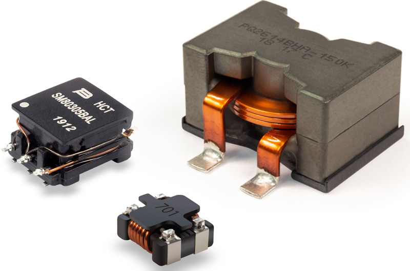
Click image to enlarge
Bourns®Model HCT transformers, Model PQ2614 SMT inductors and AEC-Q200 compliant common mode chokes are examples of components optimized to meet the isolation safety and power conversion requirements in SMPS designs
Determining the Level of Protection Needed
The typical circuit protection arrangement at the power supply input is shown in Figure 2. The overcurrent device is first so that it protects against failures of the overvoltage element as well as the rest of the power supply. This can pose a challenge to designers because lightning and other surge events will activate the overvoltage element and the resulting surge current will be passed through the overcurrent device. Therefore, a minimum overcurrent trip value will need to be specified to allow this surge current to pass without permanently taking the power supply offline.

Click image to enlarge
Figure 2: Shows the typical location for overcurrent and overvoltage circuit protection in a power supply
Overcurrent Protection
The most common overcurrent technology is a conventional fuse. There are multiple types of fuses including fast-acting, slow-blowing and high inrush current tolerant reaction time profiles to allow designers to tailor the fuse response. For designs that can benefit from circuit protection that offers series resistance to limit inrush currents, fusible resistors may be a good option.
In various power supply applications, occasional overcurrent events at the input or output port may be expected due to accidental temporary shorts and overloads. To eliminate nuisance fuse blowing, self-resetting polymer and ceramic PTC (positive temperature coefficient) devices are optimal solutions in most applications.
Overvoltage Protection
Metal Oxide Varistors (MOVs) are popular overvoltage protection solutions selected based upon their line voltage rating. Designers will typically add a safety margin to the power supply rated voltage input to allow for temporary line voltage swells. To ensure the voltage does not exceed these requirements, larger diameter MOV devices can be specified to handle and limit higher surge currents and voltage.
However, MOVs are known to degrade over time from exposure to line voltage transients. To reduce the stress on the MOV and extend its lifespan, designers can place a GDT in series with the MOV. This effectively keeps the MOV disconnected until a significant voltage surge occurs.

New hybrid protectors now integrate the GDT/MOV functionality into a single device with matched MOV and GDT ratings. For example, Bourns®IsoMOV™ protectors combine both devices to deliver an elevated level of surge protection performance, operational life and device reliability
With the availability of new fully-integrated, compact hybrid designs, power designers can get protection performance usually found in larger traditional MOV devices. This enables them to better tailor surge protection to their space requirements, and to upgrade their MOV overvoltage protection to include the benefit of GDT isolation without a PCB redesign.
In addition, bidirectional thyristors can be used to protect a power supply from damage due to an overvoltage condition on its AC input lines. Power TVS (PTVS) devices are another option that deliver the inherent reliability of a silicon solution with lower, controlled clamping voltages.
For ultra-fast and efficient in-line overvoltage protection, Bourns offers the components of a multi-stage protection circuit approach that combines a hybrid protector with a TBU® transient blocking unit device and a TISP® thyristor. This solution effectively limits voltage let-through to the power supply, but can also protect against commonly-occurring sustained overvoltage events without damage and often without interrupting the operation of the power supply.
Overtemperature Protection
The faults that trigger overcurrent and overvoltage protection can generate excess heat within the power supply. For this reason, it is recommended to implement protection circuits to shut down the supply when an internal temperature rating is exceeded. Temperature monitoring circuits designed to ensure safe operating temperatures can come in the form of both NTC and PTC thermistors, thermocouples, resistance temperature detectors (RTDs) and semiconductor temperature sensors. However, bimetals such as mini-breaker thermal cutoff devices can be used both in the temperature monitoring circuit as well as the protection circuit as they have the ability to both conduct power due to their low impedance and then to cut the power at precise, pre-programmed temperature settings.
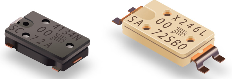
Click image to enlarge
Bourns®Model SA & SC Series mini-breakers provide the industry’s first surface mountable devices that can be PCB mounted in power supply systems
Accurate Current Measurement
Current sense resistors work by detecting and converting current to voltage. Following Ohm’s law, a voltage drop is generated across the resistor of known value, which is proportional to the current
(Vsense = I x Rshunt).
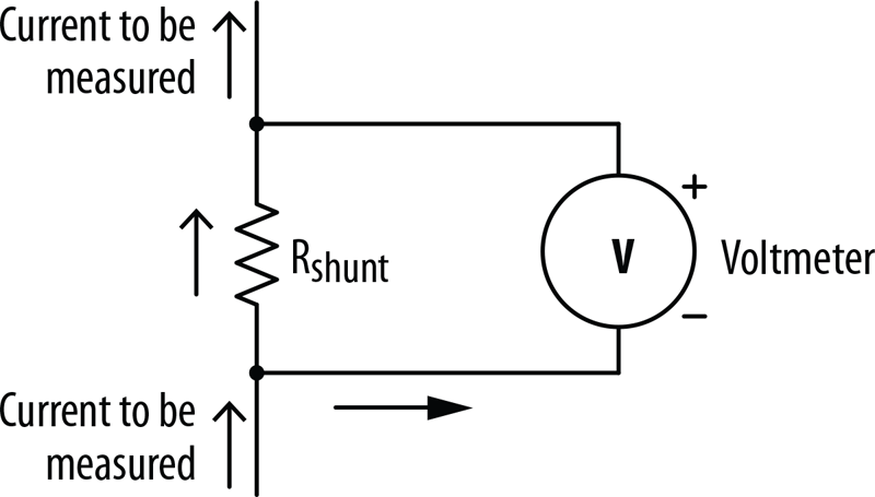
Click image to enlarge
Figure 3: A shunt resistor is placed in series with the electrical load whereby all the current to be measured will flow through it
The voltage drop across the resistor can be measured by various amplifier options such as operational, difference and instrumentation amplifiers. The signal voltage level coming from the resistor should be high enough to fit for input voltage requirements of the amplifier and must be above the electrical noise.
At the same time, however, the voltage drop on the resistor should be minimized by using the lowest possible resistance values which reduces the power loss and heat generation from the resistor (P heat = I ² x Rshunt).
For example, to sense 12 A average output when the input requirement of an IC is 30 to 130 mV, both of the following resistors can be used:
1. 10 mΩ resistor: V = 12 A x 0.01 Ω = 120 mV; P = (12 A)² x 0.01 Ω = 1.44 W.
2. 5 mΩ resistor: V = 12 A x 0.005 Ω = 60 mV; P = (12 A)² x 0.005 Ω = 0.7 W
To achieve these contradictory goals, a wide range of current sense resistors are available – from commercial and automotive grade thick film chip resistors to metal foil, metal strip and electron beam welded metal alloy shunts.
Current Monitoring and Compensation
In a flyback power structure, a current sense resistor is used to monitor switching current coming from the primary side by reading voltage across “Rs” and also provides voltage compensation to the system. The current sense resistance in a power application can range from milliohms to several ohms due to the accuracy of the controller’s ADC, which is proportional to the cost. In a power supply, resistance is also limited by the maximum current flow number, which is usually under 15 A.
In this kind of single-line current sensing, any parasitic resistance generated by PCB or by ground will tend to cause voltage deviation measured across Rs. Therefore, the tolerance of resistance is an important factor for the application. It is also important to consider the tolerance of the input signal across Rs, where the higher the power rating, the better the result.
Limiting Current and Regulating Voltage
Snubber circuits are used for switching power supplies to suppress voltage spikes helping to protect the circuit and enhance performance by reducing the power dissipation. Resistors used for snubber circuits need to be able to dissipate high peak power.
Click image to enlarge
Figure 4: indicates where a resistor is placed for primary RC snubber circuit for flyback converter
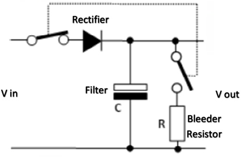
After devices are turned off, filter capacitors in the power supply circuit can still store an electrical charge. Bleeder or discharge resistors are needed mainly for safety reasons, where they are connected in parallel and discharge the energy stored in the capacitor.
Click image to enlarge
Figure 5: illustrates a bleeder resistor for discharging the capacitor of the power supply filter. Bourns®CMP Series pulse withstand thick film resistors are designed for absorb high pulse peak power. In addition, the Bourns®CRS Series pulse power resistors are tested for 1.2/50 µs surge and the Bourns®CHP Series pulse power resistors feature an extremely high rated power up to 3 W
Maximizing Power Supply Safety and Efficiency
Magnetics, circuit protection and resistor devices are fundamental component building blocks in a power supply design. This article is developed as a basic primer to help designers narrow and speed their selection of the types of components required to help meet regulatory standards while also maximizing power supply reliability, efficiency and above all, safety.