Reverse conducting IGBTs (RC-IGBTs) enable a scale-up in IGBT power rating without increasing the module or system-form-factor
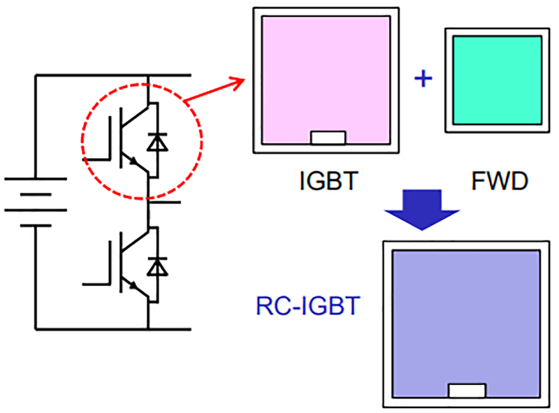
Figure 1. Diagram and equivalent circuit of the 7th generation X-series RC-IGBT technology
From electric vehicle onboard chargers (OBCs) and fast DC chargers to solar micro-inverters and larger industrial laser, welding, and automation use cases, there is a wide array of applications that rely on modern power conversion. One striking commonality between these applications is the continual push in chip design, fabrication, and packaging technologies to improve power density, thermal management, and efficiency -- all while minimizing cost.
Traditional insulated-gate bipolar transistors (IGBTs) have been ubiquitously leveraged in power electronics applications, but users looking to move up the power spectrum will typically require either the paralleling of power modules or opting for a larger, bulkier module that has a higher voltage and current rating. Both options typically lead to a dimensionally larger solution with the same or greater heat dissipation and reliability concerns.
Understanding how the limitations of traditional IGBTs can affect equipment design
IGBTs have long been one of the most popular power semiconductor switch devices in the market. These devices strike the balance between cost-effectiveness and power density. The industry has steadily improved IGBT technology in miniaturization, cost reduction, and performance. In this iterative process towards improvement, there are several outstanding design tradeoffs and bottlenecks that could potentially limit IGBT technology—any further miniaturization of the traditional IGBT module increases power density, which can cause reliability issues. The output current increase of an IGBT module causes the operational temperature of the IGBT and the freewheeling diode (FWD) to rise, also potentially causing lower module reliability.
IGBTs also often face the common issue of “snapback” of the I-V characteristic. In this phenomenon, the IGBT is triggered at a high voltage and then falls back to conduction at a lower voltage. This process is started with a small current that flows from the collector (anode) to the emitter (cathode). As this current increases, so does the voltage drop between the buffer (field-stop) region and the anode. At this point, the anode will begin injecting carriers (holes) into the drift region as there is sufficient voltage drop in this junction. Snapback will occur when the carrier concentration in the drift region is comparable to the doping concentration. This is known as conductivity modulation where the drift region resistance drops significantly causing a snapback in voltage. IGBT snapback can cause several issues, such as:
● Preventing full device turn-on
● Causing a high forward voltage drop, which may also increase conducting energy loss
● Creating a non-uniform current distribution, which can decrease the conducting capability and reliability of the device
Overcoming the challenges of traditional IGBTs with RC-IGBTs
As device designers seek more power, more performance, and more compact packaging, the solution was to look past traditional IGBTs. That’s the genesis for reverse-conducting IGBT (RC-IGBT) technology. RC-IGBTs integrate an IGBT and FWD into a single chip to reduce the number of chips and total chip area. See Figure 1. Along with this miniaturization, the RC-IGBT also exhibits improved performance.
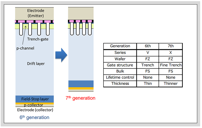
RC-IGBT chip technology enables a thinner drift layer, the miniaturization of the trench gate structure, and an optimized field stop layer. See Figure 2. This drastically reduces the collector-emitter saturation voltage (VCE(sat)). The products are formed into a thin wafer to improve the trade-off relationship with turn-off loss and VCE(sat). Typically, the utilization of thin wafer technology will have the additional consideration of voltage oscillations at turn-off and a reduction in the breakdown voltage. However, even this is improved upon through the optimization of the field stop layer—the voltage-withstanding structure on the backside of semiconductor chips. Overall, these improvements ultimately reduce inverter power losses and increase the efficiency of the end design.
Click image to enlarge
Figure 2. IGBT cross-section comparison between the older (6th) generation of IGBT and the new (7th) generation of X-series RG-IGBTs
Leverage advanced packaging technology to deliver higher power densities
RC-IGBT technology alone isn’t sufficient to provide designers with the power densities that they require. The combination of the optimized chip and package technology allows for an expanding current rating while also miniaturizing the IGBT module.
As an example, Fuji Electric’s 1,200 V 7th generation X-series module uses new materials along with an optimized bonding wire diameter for a more robust structure as well as new silicone gel solution. All of this combined enables a maximum continuous operating temperature (Tvjop) of 175oC for a higher output power without increasing the package size. For instance, the rated current of the 1,200 V PIM (Power Integrated Module) package for X-series is increased to 75A from 50A of the previous generation, this yields a 50% expansion of rated current.
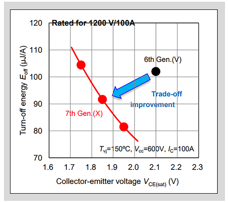
The on-state voltage drop (VCE) of the X-series RG-IGBTs is reduced by 0.25 V. As a result, power dissipation during device conduction decreases and the power conversion efficiency of the end design increases. However, this does not come with the common tradeoff of more turn-off losses. See Figure 3. In fact, the X-series turn-off energy has dropped by 10% by significantly reducing the tail current. This reduction in the tail current is achieved by employing the thinner drift layer. This chip optimization directly realizes a power loss reduction even though the chip size has been reduced.
Click image to enlarge
Figure 3. Turn-off energy(Eoff) over collect-emitter voltage (VCE(sat)). The 7th generation of RC-IGBTs shows an improvement in both Eoff and VCE(sat)
Rooting out the reliability issues of traditional IGBT modules
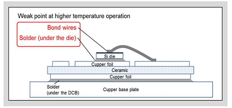
Typically, an IGBT module consists of a ceramic substrate for insulation that is soldered to a base plate that is generally constructed of copper. See Figure 4. The high heat-dissipating ceramic substrate has the biggest impact on the thermal resistance between the chip and the heat sink. Alumina (Al2O3) and aluminum nitride (AlN) ceramics are often used due to their high thermal conductivity and cost-effectiveness. However, the AlN substrate is generally thick and therefore fairly rigid. This will cause reliability issues with the solder layer under the substrate--thermal stress can cause cracks and deformations at this interface.
Click image to enlarge
Figure 4. Module structure for IGBTs.
Continuing with Fuji Electric’s 7th generation X-series module as an example, this RC-IGBT solution employs thinning of the AlN ceramic layer while maintaining good thermal resistance and material strength through optimal ceramic sintering conditions. The result is a high heat dissipation substrate that is less prone to failures due to thermal stress -- increasing reliability while decreasing module size.
Another potential failure mechanism for IGBT modules is the solder joint under the chip and the connected wire on the chip’s surface. At this joint, the mechanical strain between the two interfaces can be severe at high temperatures. The different coefficients of thermal expansion (CTE) between the surfaces directly leads to an oscillating mechanical stress at the joints. This can lead to failure. To resolve this in RC-IGBT, the 7th generation X-series modules example, utilize optimized bond wire diameter and length to ensure a sufficient power cycle withstand capability at continuous operating temperatures of 175oC.
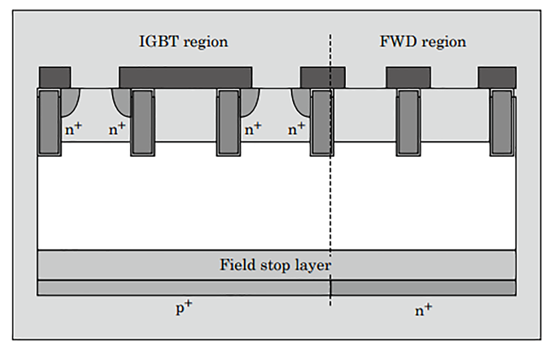
The snapback phenomenon is also resolved with RC-IGBTs by optimizing the structure of the chip. Electrons are injected into the cathode layer of the FWD region, this suppresses hole injection from the collector layer of the IGBT and hinders conductivity modulation; the prominent reason for the snapback phenomenon. See Figure 5. This greatly improves device reliability by mitigating all the negative effects of snapback.
Click image to enlarge
Figure 5. Cross-sectional diagram of RC-IGBT structure
More power. More performance. More compact packaging
In an ever more competitive design market, having to ability to reach equipment performance targets without compromise becomes even more critical. RC-IGBTs help you do just that.
Enhancements to the chip level include a thinner drift layer, miniaturization of the trench gate structure, and an optimized field stop layer. At the package level, the thinning of the AlN substrate, improvement of the Silicone gel, and the optimization of the bonding wire diameter and length all allow for device reliability at high continuous operating temperatures. The combination of all these enhancements enables higher current ratings and the miniaturization of IGBT modules. This ultimately allows the end design (e.g., inverter) to be more efficient, power-dense, and reliable while maintaining its cost-effectiveness.