Author:
Richard Houlihan, Naveen Dhull, and Padraig Fitzgerald, Analog Devices
Date
08/29/2022
 PDF
PDF
Click image to enlarge
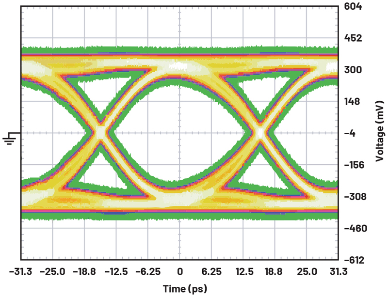
Figure 1: Eye diagram at 32Gbps (RF1 to RFC with reference trace, pattern used PRBS 215-1)
The semiconductor market is evolving with higher speed and higher density interchip communications for advanced processors. Assuring quality amidst this increasing complexity and demand for increased throughput is a challenge for today’s ATE designers. One critical aspect is the increasing number of transmitter(Tx)/receiver (Rx) channels, which require both high speed digital and DC parametric testing. These challenges are driving complexity in semiconductor tests and not addressing them leads to increased test time, increased loadboard complexity, and reduction in test throughput. In turn, this will drive up operational expenses (OPEX) and reduce productivity in a modern ATE environment.
To solve these ATE challenges, a switch that is operational at DC and highfrequencies is needed. Analog Device’s ADGM1001 can pass true 0Hz DC signals and up to 64Gbpshigh speed signals to enable an efficient single test platform (one insertion) that can be configured to test both DC parameters and high speed digital communication standards, such as PCIe Gen 4/5/6, PAM4, and USB 4.
HSIO Pin Testing
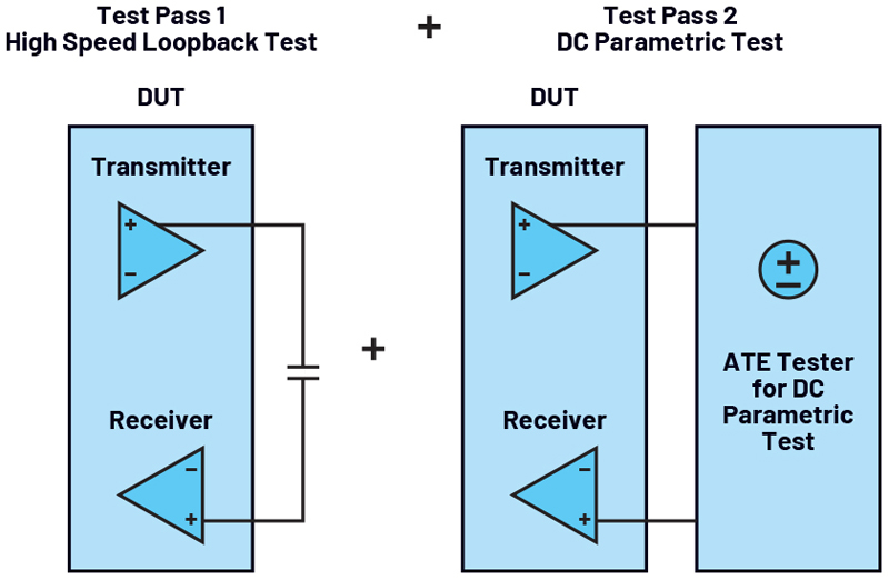
Testing high speed input output (HSIO) interfaces in a high volume manufacturing environment is a challenge. A common approach to validate an HSIO interface is to implement a high speed loopback test architecture. This incorporates both high speed and DC test paths in one configuration. To perform high speed loopback testing, generally a pseudorandom bit sequence (PRBS) is transmitted at high speed from the transmitter and received at the receiver end after being looped back on the load board or test board as shown in Figure 2 (left side). At the receiver end, the sequence is analyzed to calculate the bit error rate (BER).
Click image to enlarge
Figure 2: Illustration of a two insertion test methodology
DC parametric tests, such as continuity and leakage tests, are performed on I/O pins to ensure device functionality. To perform these tests, pins need to be connected directly to a DC instrument where a current is forced and a voltage is measured in order to test for failures. To perform both a high speed loop back test and a DC parametric test on the DUTI/Os, there are a few methods that can be used to test the digital SoC; for example, using MEMS switches or relays, or using two different types of load boards, one for high speed testing and the other for DC testing, which requires two insertions.
Click image to enlarge
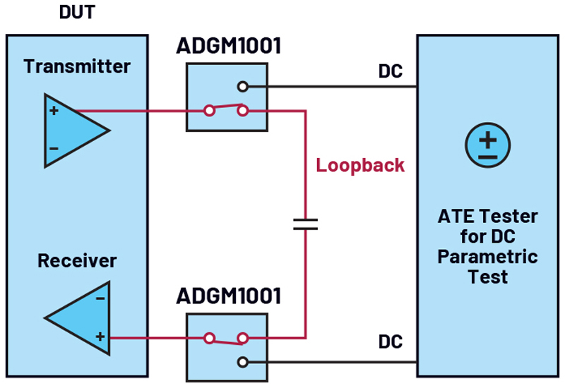
Figure 3: Enabling both high speed digital and DC testing (highlighting P channel only)
Performing high speed testing and DC parametric testing using relays becomes challenging as most relays don’t operate beyond 8GHz, so users have to compromise on signal speed and test coverage. Moreover, relays are big in size and consume a large PCB area, which impacts the solution size. Reliability is always a concern for relays as they typically only last for 10 million switching cycles, which limits system uptime and load board lifetime.
Figure 2 shows a two insertion test method to perform a high speed loop back test and a DC parametric test. The left side shows the high speed digital loopback test setup, where the transmitter of the DUT is connected back tothe receiver through a coupling capacitor. On the right side is the DC parametric test setup where DUT pins are directly connected to the ATE tester for parametric tests. Until now, it has not been possible to have both high speed loopback and DC test functionality on the same load board due to component limitations.
Challenges associated with two test insertions:
► Users must maintain and manage twosets of load boards required for DC and loopback test. This adds significant overhead, particularly when testing a high volume of parts.
► Two test insertion means every DUT must be tested twice, hence the indexing time during each test will be doubled, which ultimately increases the test cost and impacts the test throughput significantly.
► Test times can’t be optimized when two sets of hardware are involved. More cost will be incurred if a part fails the second insertion. The first insertion will have been wasted tester time.
► Since every DUT is tested twice, it doubles the risk of human error.
► The two test insertion approach involves two sets of hardware, which doubles the hardware setup time.
► The two test insertion requires more component moves. It requires moving the components between testers and potentially between test houses, creating planning and logistical challenges.
Solving the Double Insertion Problem
ADI’s 34GHz MEMS switch technology offers both high speed digital and DC testing capability with high density in a 5mm × 4mm × 0.9mm LGA package. To perform a high speed digital test, high speed signals from a transmitter are passed through the switch and routed back to a receiver, where after decoding, the BER is analyzed. For parametric DC testing, the switch connects the pins to the DC ATE tester where parametric tests such as continuity and leakage tests are performed to ensure device functionality. During parametric DC testing, MEMS switches also provide an option to communicate with ATE at high frequency, which is required in some applications.
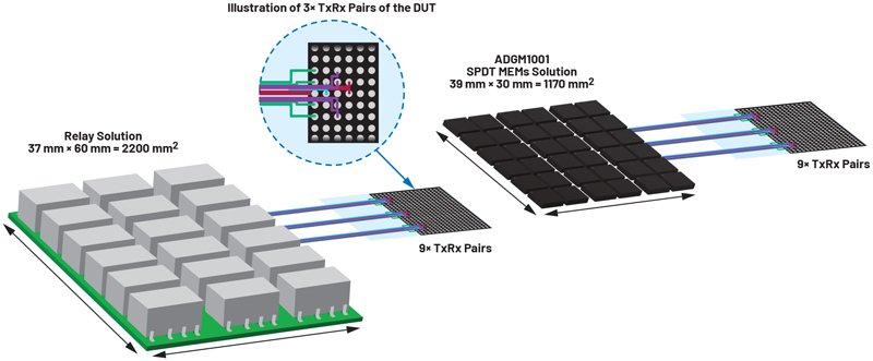
Figure 4 shows a high speed digital testing solution comparing the use of relays and ADGM 1001 MEMS switches. The solution provided by the MEMS switches is nearly 50% smaller than the relay solution. The high frequency standards such as PCIe Gen 4/5, PAM4, USB 4, and SerDes drive multiple transmitter and receiver channels, which require intense PCB densification without any layout complication to mitigate channel-to-channel variation. To meet the demand of these evolving high frequency standards, MEMS switches offer intense densification and enhanced functionality in the load board design for digital SoC testing.
Click image to enlarge
Figure 4: Comparing the loopback solution provided by relays vs. the ADGM1001
Relays are typically large and have limited high frequency performance. They struggle to support higher frequency standards such as PCIe Gen 4/5, PAM4,USB 4, and SerDes with enhanced densification. The majority of the relays don’toperate beyond 8GHz and their poor insertion loss at high frequencies impactsthe signal integrity and limits the test coverage.

Click image to enlarge
Figure 5: RF performance
Click image to enlarge
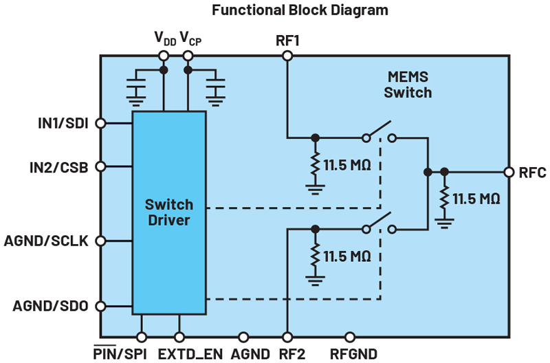
Figure 6: Functional block diagram
The ADGM1001
The ADGM1001 SPDT MEMS switch provides high performance from DC to 34 GHz. Due to the ultra low parasitics and wideband width of the technology, the switch has minimal impact on signals up to 64Gbps and offers minimal channel skew, jitter, and propagation delay enabling high fidelity data transmission. It provides a low insertion loss of 1.5dB at 34GHz and low RON of 3Ω typically. It offers excellent linearity of 69dBm and can handle high RF power of 33dBm. It comes in a small 5mm × 4mm × 0.95mm plastic SMD package, with 3.3V power supply and simple low voltage control interface. All these features make the ADGM1001 an ideal candidate for ATE applications enabling both high speed digital and DC parametric testing capability in a single test insertion.

Click image to enlarge
Figure 6: Functional block diagram
The ADGM1001 can be controlled via the logic control interface (Pin 1 to Pin 4) or via the SPI interface. All the required passive components for device functionality are integrated inside the package for ease of use and board space saving. Figure 6 shows the functional block diagram of the ADGM1001.