SAN JOSE, CALIF. – NXP Semiconductors N.V. introduced the LPC84x family, the latest addition to its rapidly expanding LPC800 series of 32-bit ARM 30 MHz Cortex-M0+ based microcontrollers. The family, designed to balance power, performance and price, addresses the growing demand to simplify and speed development — enabling smarter next-generation designs to be cost- and power-efficient.
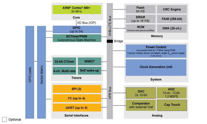
Advancing its power-efficient integration and providing increased flexibility to developers, the LPC84x family builds on its innovation with a unique way to configure the device without CPU intervention. Upon power-up, its fast access initialisation memory (FAIM) allows the clocks of the LPC84x microcontroller to be started in a low frequency mode, keeping startup current consumption to a minimum. Additionally, its input/output (IO) ports can come up immediately and in its desired configuration, eliminating any potential termination issues with attached devices, such as MOSFETs.
Within the LPC84x family, the LPC845 offers an additional flexible capacitive touch-sensing solution, which can operate in sleep and deep sleep modes, allowing for very low power performance. The LPC845 solution has been designed to handle up to nine capacitive buttons in different sensor configurations — such as a slider, rotary or a button matrix — along with supporting software libraries and tools to support additional features, including auto-calibration for best performance in noisy or wet environments, reducing false triggering. Evaluation kits and software packages available starting in Q3 2017.
Building on NXP’s global success of the LPC800 series, and keeping consistent with its proven, industry-leading innovations, the LPC84x family includes its powerful 32-bit State-Configurable Timer with PWM, advanced DMA, autonomous serial interfaces and patented IO switch matrix, where any peripheral function can be assigned to any of the 56 GPIO, enabling low-cost PCBs.
NXP’s new LPC84x MCU family offers developers a path to 64 KB of integrated flash memory and 16 KB SRAM, with a 12-bit ADC, dual 10-bit DAC, and a selectable output free-running oscillator (FRO) — further expanding the LPC800 series of feature-rich, entry-level MCUs at aggressive 8-bit pricing. Customers benefit from the family’s greater levels of integration for monitoring, data collection, sensing, real-time control and graphic interface capabilities, enabling basic control and connectivity tasks across a broad range of consumer, industrial and emerging IoT applications.
Pricing and availability
Available in a scalable family of packages, including LQFP64, LQFP48, HVQFN48 and HVQFN33, the LPC84x MCU family of devices, along with supporting peripheral drivers, example software and tools, including the LPCXpresso845-MAX development board (OM13097), are available beginning June 20, 2017.
Visit nxp.com/LPC84x for additional information of the LPC84x MCU family.
 PDF
PDF