The shrinking world of ceramics
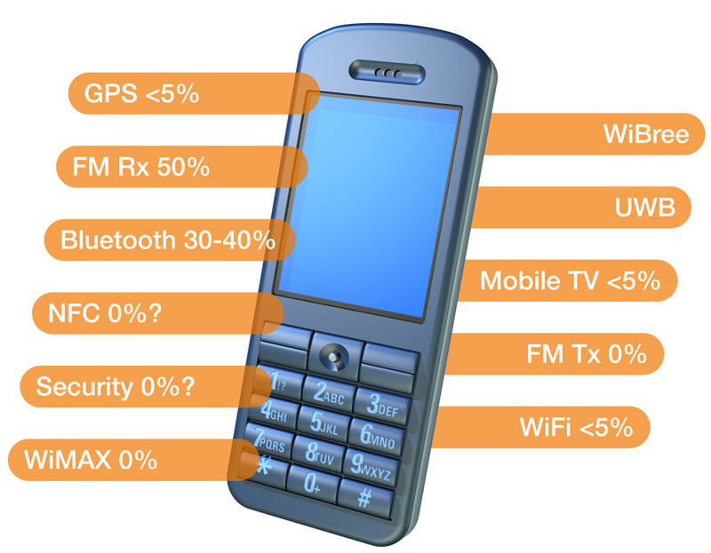
Figure 1: A wireless handset may need to cover 13MHz to 6GHz in future - figures show the Murata estimate for the take-up of various technologies
Ceramic technologies are complementing semiconductor advances in enabling ever-more sophisticated and smaller wireless electronic systems. Improvements in ceramic materials technology have led to dramatic size reductions in components and sub-assemblies in recent years. This trend is so marked that the limiting factor for some designs is not the size at which particular components are available but the ability of automatic assembly equipment to handle the smallest types. Nowhere is the demand for miniaturization more prevalent than in the design of wireless devices, both for cellular and non-cellular applications. Cellular and non-cellular wireless While many people think of wireless in terms of cellular networks, the world is rapidly becoming much more complex, both within cellular phones and due to the growing number of stand-alone wireless devices now available across a range of different applications and standards. Figure 1 shows Murata's view of the likely wireless connectivity that will appear in cellular phones over the next few years. GPS satellite, mobile television (DVB-H), FM transmitters that provide a link to car radio receivers, 802.11x WiFi transceivers, Bluetooth transceivers, wireless security keys and e-money transceivers (Near Field Communications), ultra-wideband (UWB) wireless links, Wibree, FM radio receivers, and WiMax transceivers are some of the options. That's a lot of wireless technologies, plus of course the cellular network radios themselves - which may be tri- or quad-band GSM plus UMTS. In the not too distant future, we could be looking at handsets with wireless capabilities stretching from 13MHz to 6GHz. The challenge for handset makers is get the right combination of technologies into each of their phones for the intended markets they wish to serve, without making the size, power consumption of cost of the product unacceptable. Smaller components, higher levels of functional integration and the use of hybrid modules or other building blocks all have a part to play.
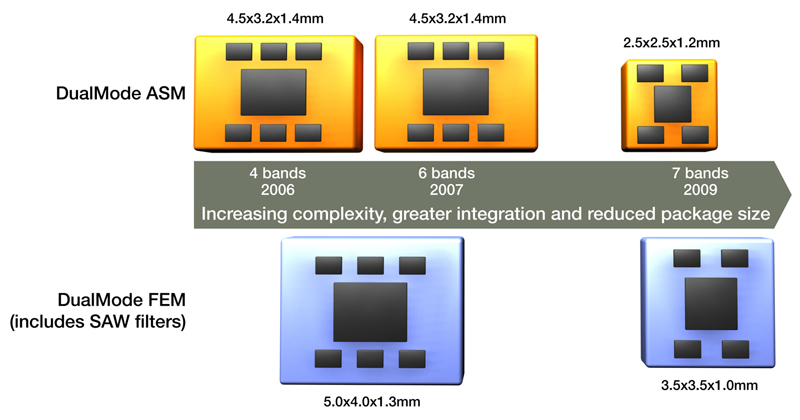
Developments in components When surface mount multilayer ceramic capacitors first became available 20 years ago the �standard' size was 1206, in other words a 3.2 x 1.6mm footprint. Today, the most common values of decoupling capacitors in RF circuits - 1000pF, 0.01μF and 0.1μF - are all available in an 0201 package measuring just 0.6 x 0.3mm - a size reduction of 96%. And at the lower end of the capacitance range, a 47pF capacitor - a popular standard value used in oscillators and filters - can be just 0.4 x 0.2mmm, the 01005 size. That's 98% smaller than its 1206 counterpart. At the other end of the scale, there are 100μF multilayer ceramic capacitors manufactured at 1206 size and components up to 47μF in the smaller 0805 size (2.00 x 1.25mm.) Of course, lower operating voltages of semiconductors have contributed to the trend for smaller passive components because dielectric layers can be thinner while still providing sufficient dielectric strength. On the other hand, the more stable dielectrics often needed in wireless applications tend to have lower dielectric constants than �general purpose' types, limiting the capacitance that can be packed into a given size. In practice, it is the challenges of component handling, inspection and re-work that limits the adoption of some of the smaller packages. At the time of writing, the cellular phone industry is in the process of moving from 0402 to 0201 for components where suitable capacitance values are available. Similar size reductions have been achieved in other passive components. Chip inductors for power supply filtering through to coils for use at microwave frequencies have been shrinking year on year. For wireless devices the 01005 package is the smallest in general use. Coils up to 120nH are available in this size, rated at 150mA, or with a self-resonant frequency of at least 600MHz. Coils up to 5.1nH have a typical self-resonant frequency of over 6GHz. As a result of these improvements, EMI filters comprising combinations of ferrites, wound inductors and capacitors, have all shrunk too. Developments in devices With respect to wireless applications, ceramic devices, as distinct from the simplest components, include dielectric antennas, connectors, piezo speakers, surface-acoustic wave (SAW) filters, isolators, ceramic resonators, ceramic duplexers and gyro sensors. In devices for combining, filtering and separating signals great advances have been made in recent years and rapid progress continues, as shown in Figure 2. Only recently, single frequency SAW filters were in an industry-standard 2.5 x 2.5 mm package - now you get the same device in a 1.4 x 1.1mm package. SAW duplexers and diplexers have followed a similar size reduction trends. Murata's Switchplexers™ are RF diode antenna switches on ceramic substrates, with integral low-pass filtering on the transmit side and a diplexer to split the GSM channels. Today, a 6-band device that will handle 3 x GSM and 3 x UMTS bands comes in a 4.5 x 3.2mm package but this is expected to become a 7 band part with its size reduced to 2.5 x 2.5mm within 2 years - no mean feat when you consider the challenges of isolating individual filters to prevent signal leakage and crosstalk between channels. These advances in ceramic-based devices are being achieved through improvements in materials technology, design and processing techniques.
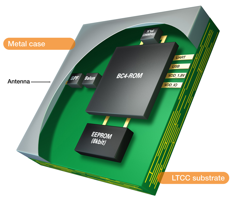
Migration to modules The growing complexity of both baseband and RF technologies within wireless systems, together with the imperative of reducing costs, is driving handset OEMs, and others, towards a platform approach to system design. Semiconductor manufacturers produce ASICs that handle various circuit functions within industry-defined standards. ASIC development within the wireless OEM companies themselves has become too expensive for most to consider, mainly due to rising costs resulting from shrinking geometries in semiconductor fabrication. Much of the differentiation of final products is created in software or through the design of system packaging. In fact, for mobile phone makers, some 80% of their design effort is now software development. This trend is further evidenced by the growth in the use of pre-assembled modules. In other words, the system designers are specifying more pre-fabricated circuit blocks in order to focus their efforts on achieving rapid time-to-market and product differentiation. In order to produce competitive modules, companies such as Murata now work as closely with semiconductor manufacturers as they do with OEMs. The design of modules and the implementation of successful reference designs based around them, means ensuring that passive components work well with their associated semiconductor devices. This has been a relatively easy task in the past but as wireless operating frequencies rise into the GHz region, even apparently simple capacitors take on greater complexity. For example, every conductor, including the component terminations, contributes inductance to a circuit and when considering capacitors, how impedance and equivalent series resistance (ESR) varies with frequency needs to be considered. At 2.5GHz 10pF capacitor from one company can be a different component to a 10pF capacitor from another - even where similar dielectric characteristics are claimed. For example, specifying a COG (or NPO) dielectric based on its stated temperature characteristics may not fully describe how the component will function in a given application. Wireless modules are assembled on ceramic substrates, so it is no surprise companies with their origins in ceramic electronic component now dominate the ceramic modules business. A well-design module based on standard low temperature co-fired ceramics (LTCC) will require only half the XY area of a conventional printed circuit board (PCB). Today, the Bluetooth transceiver module shown in Figure 3 is available in a 6.15 x 6.15mm package - complete with crystal and EPROM. 802.11B transceivers come in modules measuring 8.4 x 8.2mm. A new non-shrink LTCC technology has been developed by Murata to produce a further 20% space saving. The non-shrink substrate enables more aggressive design rules to be used, with circuit interconnect and components laid out closer together. As a result, 2008 will see a combined Bluetooth and 802.11x module appear in a tiny 10 x 10mm package. Conclusion The growth in transistor density within ICs and the capabilities of the resulting chips are well documented. Equally important, but perhaps less well appreciated, are the advances that have been made in materials and processes related to ceramic technologies. These are the technologies enabling electronic systems designers to take even greater advantage of progress in the semiconductor industry. www.murata.eu


