With new switch technologies, such as SiC or GaN, these switch transitions are particularly short
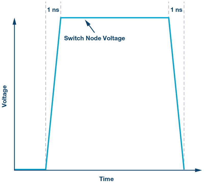
Figure 1: Rapid switching transitions cause interference
Every switch-mode regulator for voltage conversion causes interference. These are partly line-bound at the input side and output side of the voltage converter, but partially these are also radiated. Those interferences are mainly caused by the rapid switching edges. They are only a few nanoseconds long in modern switch-mode regulators. With new switch technologies, such as SiC or GaN, these switch transitions are particularly short. Figure 1 shows switch transitions that are about one nanosecond long. The underlying frequency is not to be confused with the switch frequency of a step-down regulator. However, there are ways to overcome interference problems. Switching edges, as shown in Figure 1, should be executed as quickly as possible in order to minimize switching losses.
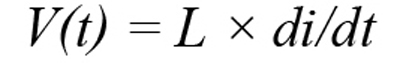
In order to create an optimized board layout in which the radiated interferences are as low as possible, the hot loops of a switch-mode regulator must be made as small as possible—that is, with as little parasitic inductance as possible. To illustrate the influence of rapid switching currents we calculate an example. If 1 A current is switched on and off within one nanosecond and there is a parasitic inductance of 20 nH in this current path, a voltage offset of 20 V is generated. This results from the formula:
The generated interference (EMI) is caused by 20 V voltage shift through the 20 nH parasitic inductance in the hot loop. To minimize this, the parasitic inductance must be kept as small as possible.
Step-down (buck) switch-mode regulators require the input capacitor to be as close as possible to the high-side switch as well as the ground connection of the low-side switch. For monolithic, synchronous step-down switch regulators, this corresponds to the connection of the input capacitor to the VIN and GND connection of the step-down regulator ICs. If these connections are made with as little inductance as possible, the generated voltage offset and, thus, the EMI are as low as possible.
Click image to enlarge
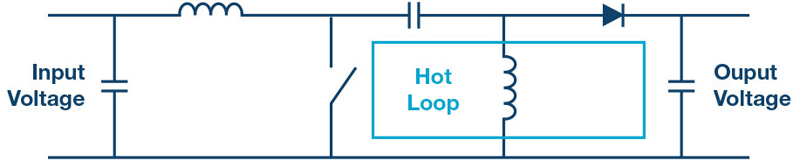
Figure 2: Critical path (hot loop) with a SEPIC converter
How does this concept behave in case of switch-mode regulators according to the SEPIC topology? The SEPIC topology is quite popular because it can generate a positive voltage from a positive voltage, which can be above or below the supply voltage. Thus, this amounts to a buck-boosttopology. Figure 2 outlines this topology. In addition to a step-down topology, a second inductor and a coupling capacitor are required.
Since a SEPIC converter is also a switched-mode regulator, the same rapid switched currents (like with a step-down converter) appear in this topology. These hot-loop current paths should be as short as possible in order to minimize the generated interference. For this purpose, each path of the step-down regulator must be considered. Does a conductor carry power continuously or only during the on or off time? In Figure 2, all lines are marked in light blue where the current flow changes with the rapid switch transitions. These paths are therefore the critical hot-loop paths and must be created with as little parasitic inductance as possible. No vias or unnecessarily long connection lines may be inserted in these paths.
SEPIC switch-mode regulators also have critical hot loops, which are essential for low EMI behavior. If these hot loops are skillfully designed with very low parasitic inductance, only a small voltage offset is generated, resulting in less radiated interference. With SEPIC switch-mode regulators, it is not the input capacitor that is so critical, as with the step-down switching regulators, but the current paths as described in this article and shown in Figure 2.
Analog Devices