Modeling Common Topologies with Silicon Carbide MOSFETs
Now more than ever, engineers are choosing Silicon Carbide (SiC)-based products for their higher efficiency, power density, and better overall system cost
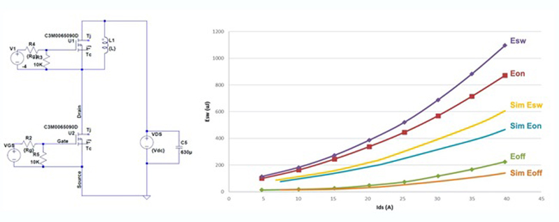
Figure 1: Ideal double-pulse test simulation switching loss results are about 45% lower than those in the datasheet for the DUT, U2
Beyond the basic design principles common between SiC and Si, and the need to keep in mind SiC’s different characteristics, capabilities and advantages, engineers must model and simulate to ensure they will meet their design goals.
As with Si, SiC now has optimized tools and models available from various suppliers, and standard modeling mitigations can be applied. While there are differences between tools like LTSpice, PLECS, and Wolfspeed’s SpeedFit 2.0 Design Simulator, tips from Wolfspeed’s Power experts will help achieve simulation accuracy with SiC.
Static simulation with LTSpice
Wolfspeed’s Spice models are optimized for 25ºC and 150ºC. The body diode operation is optimized for a drive voltage, VGS, of -4 V for Gen. 3 devices and -5 V for Gen. 2. Engineers can incorporate self-heating and transient thermal capability, and parasitic inductance. However, parasitic bipolar and associated effects, avalanche multiplication process, and variation of body diode turn-on voltage with gate-to-source are not modeled.
LTSpice static simulation results – the IV curve at various VGS values and the body diode curve – match up well with actual measurements. For capacitances – input capacitance, Ciss, output capacitance, Coss, and reverse transfer capacitance, Crss, too, the static simulation results are fairly close for the purpose. Engineers can therefore feel confident in the static parameters of the Spice modeling.
A double-pulse test
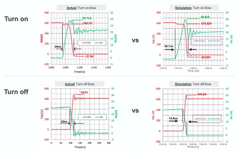
A typical characterization benchmark for understanding dynamic behavior is a half-bridge double-pulse test. When modeled without any considerations, such as parasitics, the simulation is significantly off the measured results (figure 1). Since energy consumption impacts efficiency, such a big difference has a significant effect on thermal calculations.
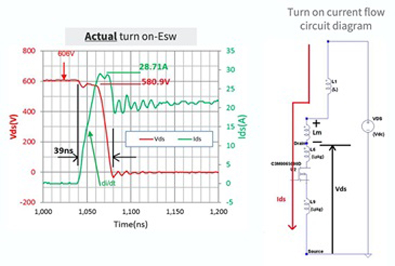
In the test case, a long pulse is followed by a 1 µs gap, which is followed by short pulse. Turn-on and turn-off are measured in the conventional way as one would with Si-based devices. Taking a closer look at the waveforms (figure 2) highlights the difference between actual and ideal simulated results.
Both rise and fall times in the simulation are much faster than those measured because the actual results are affected by inductances – parasitic stray inductance, Lm, between the two devices, and package inductance, Lpkg, which is the source inductance of the package. There is also a difference between overshoot results for turn-on and turn-off. These differences contribute to the overall difference in switching losses.

Click image to enlarge
Figure 2: A comparison of the waveforms reveals that the actual turn-on rise time is 39 ns vs a much faster 22.83 ns simulated and the actual fall time is 20 ns vs simulated 13.63 ns
To get an accurate model, the inductances must be extracted and manually imported into LTSpice. Thermal model in PLECS, on the other hand, does not include parasitic components.
Click image to enlarge
Figure 3: Information extracted from the actual waveform can be used to compute Lm
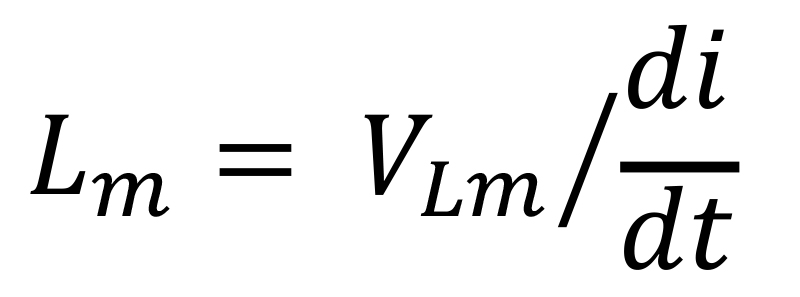
Finding Lm
Lm is the inductance between the source of the high-side U1 device and the drain of the low-side U2 device. Although it can be directly measured, it can also be extracted thus (figure 3):
Where:
VLm = Vin – Vds, and from the example,
di/dt = 1.105 x 10⁹,
Vin = 606 V, and
Vds = 580.9 V
This gives a value of 23.1674 nH for Lm.
Whether it is a synchronous buck, synchronous boost, half-bridge or full-bridge, the design likely uses a configuration of high-side and low-side devices through a PCB. If good layout practices are followed, Lm is in the 20 nH-to-25 nH range. Engineers can regard that as a rule of thumb to use in simulations.
Extracting Lpkg
Designers might expect Lpkg to be the same across suppliers for standard packages like the TO-247. However, there are variations due to the differences in the thickness of lead frames, in source wire bonding, and in the length of the shoulder on the package. If available in a datasheet, it can easily be plugged into the model. If not, it can be extracted from a measured waveform and extrapolated to what might be a good estimate for the package at hand.
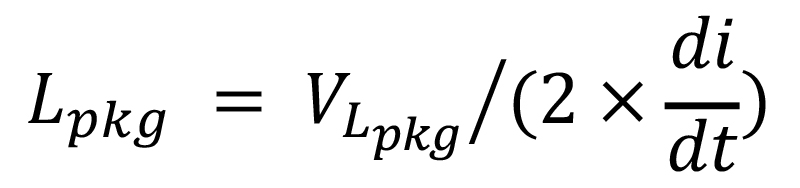
Where:
Lds = 6.5372 nH from the Spice model,
Vds = ~-27.8 V from the actual waveform,
VLds = -15.035 V,
Vds_on @ 20 A = 1.25 V from the C3M0065090D datasheet, and di/dt = -2.3 x 10⁹
di/dt = -2.3 x 10⁹
Click image to enlarge
Figure 4: Adding the computed inductances into the LTSpice model brings it close to the actual measurements
In our example, this gives an Lpkg value of 2.503 nH. Despite variations, this value can be taken as a good estimate and a reliable rule of thumb. Simulating after taking the inductances into account makes the dynamic model accurate (figure 4).
With the inductances factored in, total switching energy Esw as well as Eon and Eoff for actual and simulated double-pulse test become very close
Using these rules of thumb for Lm and Lpkg, engineers can get fairly accurate loss and thermal calculations for their thermal budget.
Paralleled MOSFETs
SiC MOSFETs are often placed in parallel to increase the current-carrying capability as well as power levels. There are some considerations to bear in mind, however:
· Current imbalance due to threshold voltage, VTH, differences
· Current imbalance due to asymmetrical parasitic inductances
· Gate drive oscillation
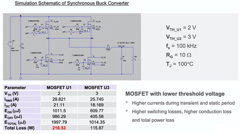
With Wolfspeed SiC MOSFETs, there is little chance of mismatching device characteristics. However, engineers may be required to use other SiC parts with a wider tolerance of specification and may choose, say, a device with 2 V VTH and another with 3 V. The device with the lower threshold has a higher transient and because of that, higher switching losses and higher conduction losses, thus higher total power losses (figure 5).
Click image to enlarge
Figure 5: The total loss of the 2V device are nearly twice those of the 3V device because of the current imbalance
Although both devices have the same gate resistance, RG, and are operating at the same temperature and switching frequency, modeling without any considerations results in U1 having over 200 W total losses and U3 just over 100 W. Simulated waveforms show that U1 peaks to about 70 A overshoot before falling to steady state of 50 A, whereas U3 peaks to about 49 A and settles to 30 A steady state. There is therefore a considerable mismatch in current carrying capability between the two devices as well as slight differences in turn-on and turn-off times.
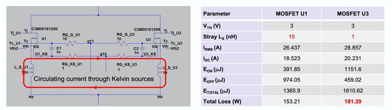
The second cause of current imbalance is asymmetric parasitics. Consider two devices, U1 and U3 (figure 6) that have the same VTH but different source inductances. This causes considerably unbalanced di/dt’s, voltages across the stray inductances, gate drives, and drain currents. Simulated waveforms show that the current ramps up and down much faster for U3, and reaches higher values for IDC and IRMS, causing 17.9% higher switching loss and 18.3% higher total loss in that MOSFET.
Click image to enlarge
Figure 6: The difference in the stray inductance Ls for U1 and U3 is exaggerated in this example to demonstrate the impact of mismatch
Increasing tool choice
SiC-based designs can be modeled using Wolfspeed’s SpeedFit, LTSpice or PLECS. Whereas SpeedFit and LTSpice can be used freely by registering with Wolfspeed, PLECS comes with a subscription fee. The differences between the tools affects both the manner of generating simulations and their limitations, such as in handling parasitics and computation of losses.