Monolithic Driver and DrMOS Technology Improves Power Design
A way for power-hungry data centers to save energy and cost, while reducing or even eliminating thermal management and EMI troubles.
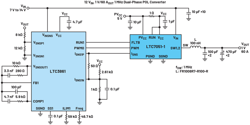
Figure 1: Dual-phase POL converter
Through the advancement of technology, microprocessors have become denser and faster on a horizontal scale thanks to the multicore architecture. Thus, the corresponding power required by these devices has increased drastically. Such power for microprocessors is provided by a voltage regulator module (VRM).
There are two main parameters driving the development of voltage regulators in this field. First is the power density (power over unit volume) of the voltage regulator, which must be increased sharply to meet the high power requirement of the system in a limited volume of space. The other parameter is power conversion efficiency for reduced power losses and better thermal management.
As developmental challenges continue to evolve, the power industry will find ways of satisfying the consequential requirements. One solution incorporates an advanced switching MOSFET, which is a major building block of voltage regulators, and its corresponding driver in a single, monolithic die along with advanced packaging, enabling compact and efficient power conversion. These DrMOS power stages have optimized high speed power conversion.
As the demand for these power stages, known as smart power stages, increased steadily and power-switching technologies continued to advance, Analog Devices came up with its version of DrMOS smart power modules. The LTC705x DrMOS series makes use of ADI’s Silent Switcher 2 architecture, along with an integrated bootstrap circuitry, which allow the DrMOS module to switch at an ultrafast speed with reduced power losses and switch-node voltage overshoot for improved performance. LTC705x DrMOS devices also offer safety features such as overtemperature protection (OTP), input overvoltage protection (VIN OVP), and undervoltage lockout (UVLO) protection.
LTC7051 Silent MOS Smart Power Stage
The LTC7051, a member of the LTC705x DrMOS family, is a 140A monolithic smart power module that successfully combines high speed drivers with high figure of merit (FOM) top and bottom power MOSFETs and a comprehensive monitoring and protection circuitry in one electrically and thermally optimized package. Together with a suitable PWM controller, this smart power stage provides the industry’s highest efficiency, lowest noise, and highest density power conversion available to the market. This combination equips a high current voltage regulator module with the latest techniques on efficiency and transient response. The typical application of LTC7051 is illustrated in Figure 1. It functions as the main switching circuitry of a buck (step-down) converter in conjunction with theLTC3861 dual, multiphase step-down voltage mode DC-to-DC controller with accurate current sharing.
To demonstrate the key features of LTC7051, ADI created an evaluation board to showcase the performance of the LTC7051 vs. a product available from the competition. Such a demonstration platform facilitates a nonbiased, accurate way of comparing essential parameters such as efficiency, power loss, telemetry accuracy, thermal, and electrical performance of LTC7051 DrMOS with those of a competitive product. The objective of the comparison was to remove any doubt on the validity of the outcome. The said demonstration platform was used to highlight best-in-class DrMOS performance metrics regardless of the manufacturer.
DrMOS Analysis Evaluation Hardware
The analysis demonstration hardware has the following key features:
• A PWM controller that can operate on a wide range of input and output voltages and switching frequencies. In this application, the controller is LTC7883, a quad output polyphase step-down DC-to-DC voltage-mode controller, shown in Figure 2.
• Identical power stage design for both the LTC7051 and competitor devices.
• LTpowerPlay power system management environment for comprehensive telemetry of system performance provided by the LTC7883.
• Can withstand extended ambient temperature in accordance with the specified operating temperature range of both ADI and competitor devices.
• Board is designed for easy thermal capture and measurement.

Click image to enlarge
The DrMOS analysis demonstration board was carefully designed to include the key features previously mentioned. Components are symmetrically and systematically placed across each power rail and have the same PCB size and area to limit discrepancies between the power rails. Layout routing and layer stack-up are done symmetrically as well.
DrMOS Analysis Testing Methodology and Software
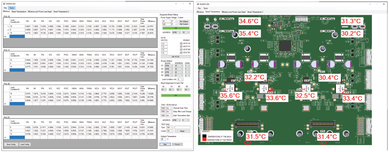
Aside from the demonstration board itself, test setup and testing methodology are equally important for unbiased data and results. For this purpose, the team also created a complementary evaluation software with a graphical user interface (GUI) shown in Figure 3 for a more user-friendly approach of testing and data gathering. The user just needs to specify input and output parameters and the software will take care of the automated testing. The software automatically controls the corresponding test and measurement equipment such as the DC supply, electronic load, and multiplexed data acquisition device (DAQ) to measure temperature, current, and voltage figures directly from the demo board, and then plot those measurements on the GUI. Important telemetry data from on-board devices are also gathered by the software through PMBus/I2C protocol. All this information is important in comparing system efficiency and power losses.
Click image to enlarge
Figure 3: DrMOS evaluation software, showing the configuration and thermal analysis tab
Data and Results
The following test results cover the steady-state performance measurements, functional performance wave forms, thermal measurement, and output noise measurement. The demonstration board was tested with the following configurations:
• Input voltage: 12 V
• Output voltage: 1 V
• Output load: 0 A to 60 A
• Switching frequency: 500 kHz and 1 MHz
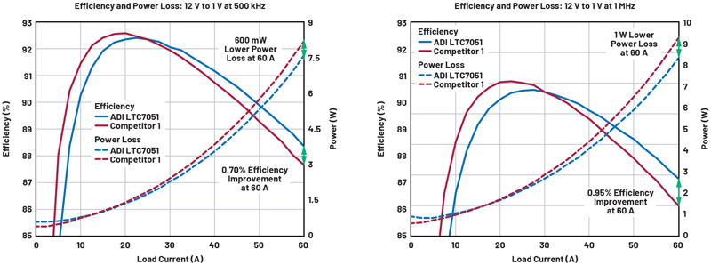
Efficiency and Power Loss
The test result in Figure 4 shows that, at a switching frequency of 500 kHz, the LTC7051 managed to have higher efficiency (0.70% better) compared to its competitor. With a further increase in switching frequency from 500 kHz to 1 MHz, the LTC7051 also provided better efficiency (0.95% greater).
Click image to enlarge
Efficiency Performance
Noteworthy here is the higher efficiency performance of the LTC7051 over the competitor at high output load current and at elevated switching frequency. This is the benefit of ADI’s patented Silent Switcher technology where improvements in both switching edge rate and shorter dead-times reduce total power losses. This enables higher switching frequency operation for a smaller solution size without a significant impact in overall efficiency. With lower total power loss comes lower temperature operation for higher current outputs, thereby significantly increasing power density.
Thermal Performance
Advantages in efficiency and power losses brought about by LTC7051 also translate to its better thermal performance. A temperature difference of approximately 3°C to 10°C was observed between the LTC7051 and the competitor offering, with the former being cooler. That better performance of LTC7051 is due to its well-designed, thermally enhanced package.
With increased ambient temperature from 25°C to 80°C, the temperature difference observed between LTC7051 and its competitor widened to approximately 15°C, with the former again being cooler.
Device Switch Node Performance
The LTC7051 drain-to-source voltage (VDS) peak is less than that of thecompetitor’s device. Also, with the load increased to 60 A, VDS measured on the competitor’s part is at its peak while prolonged oscillation can be seen. The LTC7051, on the other hand, managed to have a smaller spike and reduced oscillation, again due to the Silent Switcher 2 architecture and integrated bootstrap capacitor inside of LTC705x DrMOS family. This will translate to lower overshoot on the switch node, meaning reduced EMI, as well as radiated and conducted noise, and higher reliability as switch-node overvoltage stresses are reduced.
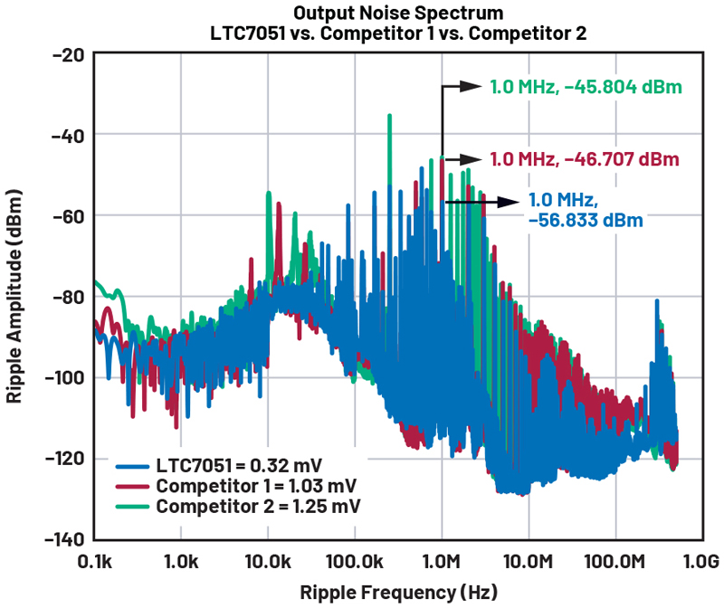
Device Output Ripple Performance
Another parameter is the output voltage ripple. The noise exhibited by LTC7051 is less compared to that of the competitor’s part. Reduced noise is due to the lower VDS spike and minimal oscillation on the switching node, which are the result of Silent Switcher technology. If switch-node spikes are not generated, then there is no conducted noise to the output.
Click image to enlarge
Figure 5: Output noise spectrum response at 1V having 60A load running at 1MHz switching frequency
Likewise, the LTC7051 and the competitor device were also subjected to output noise spread spectrum measurements as shown in Figure 5. LTC7051 outperformed the other DrMOS device, and showed that the noise generated at the switching frequency is lower compared to that of the competitor’s part. The noise difference was approximately 1 mV rms.