More Bang for Your Boost
Driving Heavier Loads with Lower Battery Voltages
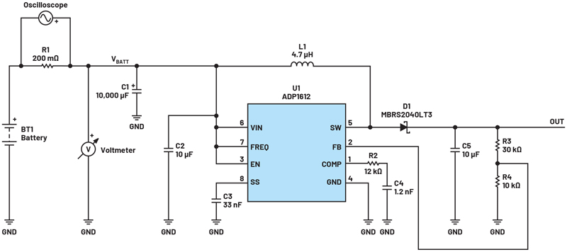
Figure 1. Evaluation kit of the ADP1612
The ADP1612 is a low-cost, high-efficiency boost converter that operates at 1.3MHz. It has a shutdown pin that reduces the quiescent current to less than 2 μA and operates with an input voltage down to 1.8 V making it ideal for battery-powered electronics. However, as the battery voltage drops, its peak current falls. This can be a benefit if the battery needs to be treated gently in its last hours, but this can also lead to problems driving heavy loads with a low battery input. Bootstrapping overcomes this problem and provides high output current with high efficiency while it allows the battery voltage to run down to a much lower level.
More battery life from a boost converter
Figure 1 shows the standard evaluation kit for the ADP1612. A 200 mΩ current sense resistor was added in series with the battery input to measure the input current. A large electrolytic capacitor was added to the battery input of the circuit to smooth the inductor’s current peaks so that average battery current could be measured across the sense resistor with a high degree of accuracy. The battery voltage was measured with a digital voltmeter and, hence, the input power could be calculated by multiplying battery voltage by input current. Resistive loads were added to the output and the efficiency of the converter was calculated by dividing output powerby input power.
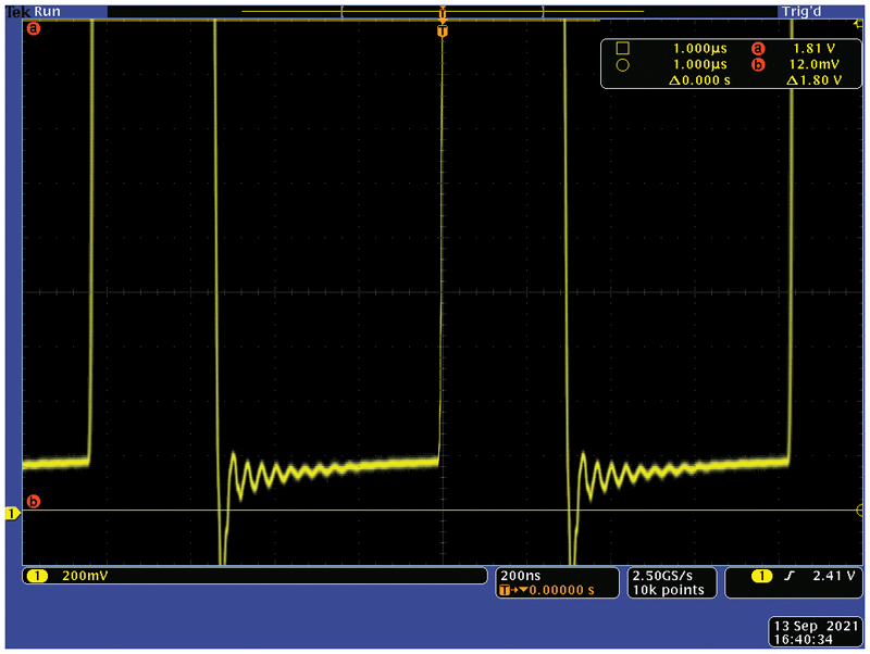
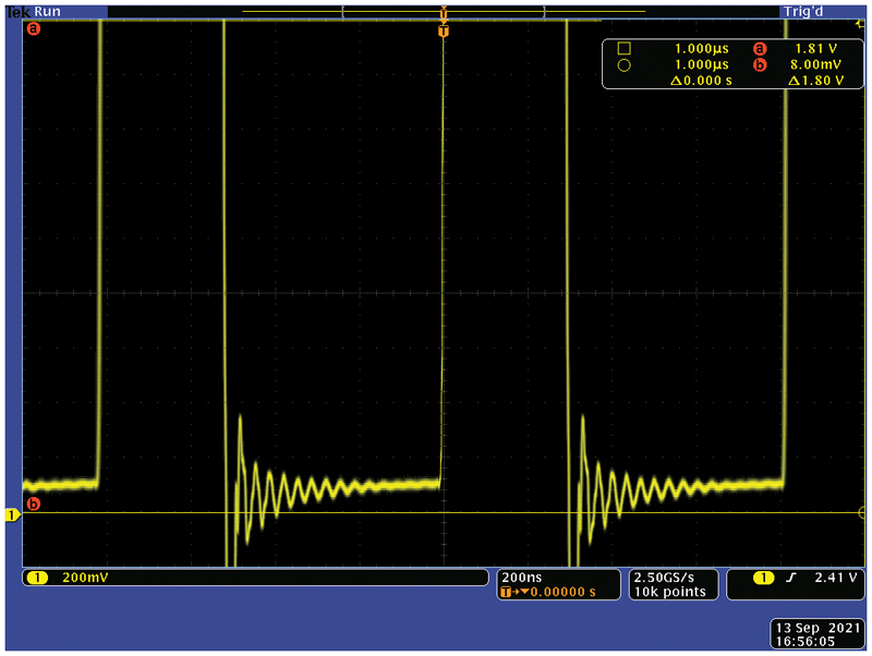
When the FET is switched on, the inductor current ramps up causing the bottom of the switch node voltage to ramp, proportional to the FET’s ON resistance. The lower this voltage, the lower the ON resistance of the FET. Hence, the lower the losses in the FET for a given current. Figure 2 shows the switch node, in non-bootstrapped configuration, with a 2V battery voltage. The bottom of the switch node voltage shows a peak value of about 180 mV.
Click image to enlarge
Figure 2. Switch node voltage, 2 V input, non-bootstrapped
Increasing the battery voltage to 3V gives the switch node waveform shown in Figure 3. Here we notice the duty cycle has gone down due to the higher battery voltage, but also that the low part of the switch node voltage is at a noticeably lower level, peaking at about 80mV. However, since the FET current with a 3V battery voltage is lower than that with a 2V battery voltage, it is difficult to see if the ON resistance has indeed reduced.

Click image to enlarge
Figure 3. Switch node voltage, 3 V input, non-bootstrapped
The circuit in Figure 1 was then converted to the bootstrapped configuration. Bootstrapping involves connecting the VIN pin of the ADP1612 to the output voltage. Once the part has started up, it is powered from the higher output voltage, therefore producing a higher drive to the FET while the ADP1612 is unaware of the battery voltage level.
Click image to enlarge
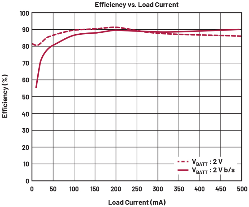
Figure 4. Efficiency of the ADP1612 with a 2 V input in non-bootstrapped and bootstrapped (b/s) configurations
The Enable pin can either be connected to the battery voltage, VBATT, or the output voltage. Connecting it to the battery voltage asserts the undervoltage lockout (UVLO) if the battery voltage goes below approximately 1.7V, while connecting it to the output voltage allows the ADP1612 to keep switching even when the battery voltage has run down to a voltage much lower than this.
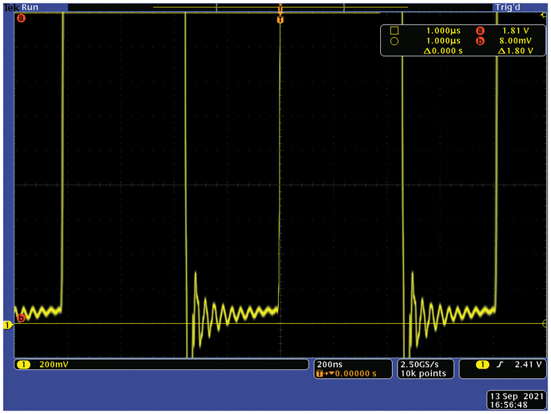
Figure 5 shows the efficiency results for the non-bootstrapped and bootstrapped configurations with a battery voltage of 2 V with a measured output voltage of 4.95 V.
Click image to enlarge
Figure 5. Switch node voltage, 2 V input, bootstrapped
The efficiency curve of the bootstrapped configuration is represented by the solid line in Figure 5 and is noticeably lower at light loads. This is mainly because the quiescent current of the device (about 4 mA) now comes from the output voltage and is effectively multiplied by the factor.

We can also see that the bootstrapped circuit starts to offer an efficiencyimprovement for heavy load currents (above about 260 mA) when operated withalow battery voltage due to the higher FET drive.
Figures 6 and 7 show the bottom of the switch node voltage in bootstrapped mode. It is important to note that bootstrapping only affects the supply voltage to the controller IC. It does not affect the power path (inductor and output diode). Therefore, we can now directly compare the 2 V bootstrapped and non-bootstrapped switch node voltages (in Figure 6 and Figure 2) and the 3V bootstrapped and non-bootstrapped switch node voltages (in Figure7 and Figure 3).
Click image to enlarge
Figure 6. Switch node voltage, 3 V input, bootstrapped
There is a clear advantage to bootstrapping with low battery voltages. With a 2V battery voltage, the non-bootstrapped switch node voltage peaks at 180mV compared to only 100 mV for the bootstrapped circuit, indicating a lower ON resistance FET and consequently lower losses. There appears to be little, if any, improvement in the bootstrapped circuit with a battery voltage of 3V, with both switch node waveforms peaking at about 80 mV.
Click image to enlarge
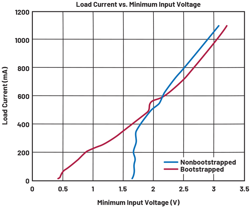
Figure 7. Load current vs. minimum input voltage
How low?
Another useful experiment is to see how low the battery voltage can be taken before the output voltage starts to lose regulation.
In the non-bootstrapped circuit, we see the UVLO circuit activates with battery voltages below about 1.7 V as shown by the blue curve. By contrast, the bootstrapped circuit ties both the Enable and VIN pins to the output voltage (5V), thus defeating the UVLO and allowing the circuit to run down to a much lower voltage. However, the circuit cannot create power from nowhere. The ADP1612 has a peak current limit; therefore, the higher the load current, the higher the battery voltage needs to be to furnish that load current for a fixed peak switch current.
The minimum operating voltage is determined by the maximum duty cycle of the converter, which is about 90%. From the equation, a 5V output and a maximum duty cycle of 90% dictate a minimum battery voltage of 0.5V, which agrees with the results shown in the graph.

Other benefits and drawbacks
The bootstrapped configuration also has an impact on the start-up voltage of the circuit. Now the VIN pin of the ADP1612 is powered from the output, the battery voltage needs to be higher than the non-bootstrapped circuit by one Schottky diode drop. The voltage drop across a Schottky diode varies with current from about 100mV (at a current of 50μA) to above 200mV at higher currents. It was found through experimentation that the start-up voltage of the non-bootstrapped circuit was about 1.75V (equal to the UVLO threshold) while this rose to about 1.95V for the bootstrapped circuit.
Conclusions
A non-bootstrapped circuit can supply a higher load current than the bootstrapped circuit with battery voltages above 2.2V. This is because the quiescent current of the ADP1612 is higher in bootstrapped mode as it is running from the output voltage. The ADP1612 also has an efficiency less than 100%, thus further increasing the required input current to the circuit for a given load current. This results in a slightly higher required input voltage in bootstrapped mode compared with non-bootstrapped mode.