MOSFET Selection and Efficiency Measurement for AI Server Power Supplies

Data centers face scrutiny over energy use, which is rising with growing demands and AI integration
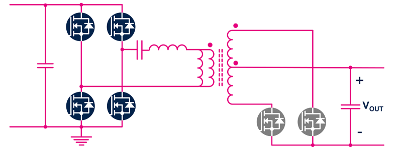
Figure 1a: Bridgeless totem-pole PFC
Yole predicts AI data center server power ratings will jump from 15kW to over 100kW, and the main bus voltage will increase from 400V to 800V to reduce distribution losses. Despite this, rack space and PSU form factors will remain unchanged, pressuring PSU vendors to achieve higher power density. Yole forecasts that 3kW PSUs with 32W/in³ density must evolve to over 10kW, implying 100W/in³.
Regulators are enforcing stringent efficiency standards, like the EU's adoption of the 80 PLUS framework. The 80 PLUS Titanium standard requires over 90% efficiency from light to full load and a minimum power factor of 0.95, necessitating active PFC. Data centers consumed 4.4% of U.S. electricity in 2023, expected to rise to 6.7%-12% by 2028 due to AI and cloud computing.
To meet demands for power delivery, efficiency, and density, designers are adopting advanced PFC and regulator topologies such as interleaved boost converter, 3-level Vienna rectifier PFC, bridgeless totem-pole PFC, and multilevel A-NPC (800V). Preferred DC-DC converter topologies include full-bridge LLC, phase-shift full bridge, and DAB, with synchronous rectification in the low-voltage output stage to boost efficiency. The choice of power semiconductor technologies for each stage is crucial for optimizing efficiency, power density, and cost.
Server Power Topologies
Figures 1a and 1b show a switched-mode power supply for high efficiency and power density, using bridgeless TTP PFC and a half-bridge (HB) LLC converter. To increase power levels, interleaved totem pole or three-phase topologies like the Vienna rectifier are needed. For DC-DC, full-bridge LLC, phase-shift, or Dual Active Bridge (DAB) topologies are recommended.
The totem pole topology enhances efficiency, reducing conduction losses by eliminating the diode rectifier that is present on the standard PFC boost, with MOSFETs in the low frequency leg (light blue devices on Figure 1a). To significantly reduce the recovery of the body diode, the high-frequency leg (green devices on Figure 1a) is made up of wide-bandgap devices achieving higher switching frequencies, leading to smaller and lighter passive components. The LLC converter's zero-voltage switching (ZVS) minimizes switching losses, allowing higher operating frequencies and smaller components, thereby increasing power density. Sinusoidal current and soft switching reduce electrical stress and EMI. The high efficiency of the LLC converter also reduces heat dissipation, easing data center cooling.
The LLC resonant converter uses a transformer with a center-tap for full-wave rectification (Figure 1b). A smart gate driver, chosen for having a control scheme suitable for this configuration, manages a pair of low-voltage MOSFETs operating in synchronous rectifier mode. The driver produces two high-current gate signals, each having 1A source and 3.5A sink current and capable of driving one or more N-channel power MOSFETs. Each gate driver has a separate control, and an interlocking logic circuit prevents the two synchronous rectifier MOSFETs from conducting simultaneously.
Click image to enlarge
In the synchronous rectifier circuit, the operating principle is to replace the power rectifier or Schottky diode with a controlled MOSFET to avoid the relatively large losses associated with the diode forward voltage (VF).
Power Choices for Resonant Converters
In general, for high-efficiency resonant converters working in ZVS, the MOSFET threshold voltage should be optimized to reduce switching-off losses. For topologies like the half-bridge LLC shown in figure 1b, keeping dv/dt within a safe operation area is important, especially during start-up and sudden load changes, where the device can work in hard-switching condition. Also, the body diode should have low values of reverse-recovery charge (Qrr) and, of course, low RDS(ON) is needed to avoid conduction losses at high loads. To reach these requirements, fast-recovery diode STPOWER MDmesh™ DM xseries can be chosen for their high dV/dt ruggedness and low recovery charge and time. An alternative is to use wide-bandgap devices.
Note also that ensuring low losses in the output capacitance (Coss) can improve system efficiency at light loads and no load. Light-load efficiency is gaining importance in server equipment designed to meet 80 PLUS Titanium, due to the extra demand for efficiency to be above 90% at 10% load.
Wide-Bandgap or Superjunction
Building on these topology choices, selecting a suitable power switch is critical to meet the performance and power density demands for AI servers. On the one hand, wide-bandgap technologies like gallium nitride (GaN) and silicon carbide (SiC) are known for their fast-switching performance and low losses, exceeding the capabilities of conventional silicon devices. On the other, the performance of silicon superjunction MOSFETs compares favorably, and devices are available at a competitive price.
The latest developments in superjunction MOSFETs are continuing to unleash more performance, making these devices a strong choice for high-power applications like AI server SMPS. Devices in the market today cover a wide range of breakdown voltage, as well as increasingly smaller RDS(on) with values of tens of mΩ.
In the PFC circuit suggested, 600V/650V superjunction MOSFETs can be used in the low frequency legs. Wide-bandgap devices are recommended for the high-frequency legs, due to their superior recovery charge performance.
The improvements in superjunction process technologies aimed at delivering faster reverse recovery in the body diode, such as with lifetime-reducing platinum diffusion, have closed the gap to wide-bandgap devices in terms of QRR performance. However, this performance is not enough to put them on the high-frequency leg of the totem-pole PFC.
Quantifying Transistor Losses on Totem-Pole PFC
It is necessary to differentiate between the low-frequency leg and the high-frequency leg. The MOSFETs of the low-frequency leg switch at the mains frequency. The only losses are due to conduction and can be calculated using the first Ohm’s law:

As regard the high-frequency leg MOSFETs, it is necessary to divide the losses during operation as boost switch and as boost rectifier, depending on the half-period of the mains voltage. These switch at several tens of kHz, and other loss contributions act on them in addition to those due to conduction. When the devices act as boost switches, they are also subject to turn-on and turn-off losses. This contribution can be calculated measuring the drain current and voltage during commutation:

When the devices act as boost rectifier, the body-diode MOSFET conducts twice inside the high-frequency period, during dead-time (tdt) and its losses are calculated by:

|
Independently of the half-period, another contribution is the gate drive losses, calculated by:

Quantifying Transistor Losses on LLC stage
Also in this case, most losses are associated with conduction, particularly at high load, although additional contributions are present.
During the dead time (tdt), the diode conducts, and the power lost in this period is:

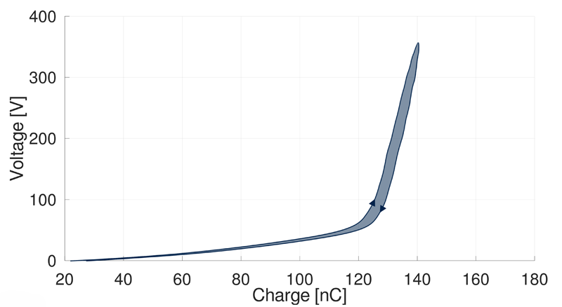
Also, in this converter the drive losses are calculated using (4). During switching, the LLC primary devices show an unwanted behavior during the charge and discharge of the output capacitance Coss. The charge moved during the two paths is different, causing a hysteresis (Figure 2). This effect is only noticeable in resonant converters with ZVS. In hard-switching topologies, the energy stored in Coss is completely lost. However, in ZVS, almost all stored energy will return to the rest of the circuit and the remaining part is lost due to the hysteresis.
Click image to enlarge
Several methods are available to quantify this contribution, although taking the necessary measurements during the functioning of the MOSFET is difficult. For this reason, a thermal method can be used.
Low-Voltage Synchronous Rectifier
Themain power losses in the SR stage are incurred while the MOSFET is in the on-state.These losses are calculated using formula
Pcond can be considerable at low voltage and high output current. Hence a MOSFET with very low RDS(ON) is desirable.
To properly switch the SR MOSFETs, without overlaps, a dead time, tdt ,is necessary. During this time, the current flows in the body diode and the losses depend on the direct voltage VF of the intrinsic diode as well as the output current, the switching frequency, and the duration of the dead time. Setting the shortest feasible dead time helps to minimize the body-diode conduction losses.
Although switching losses are low relative to conduction losses, the body-drain diode recovery time, the intrinsic output capacitance, and the gate charge are the main parameters influencing performance and power losses during switching:
At body diode turn-off the minority charge stored on both sides of the device’s PN junction must be removed before the maximum voltage is sustained (secondary voltage, VS). The power loss due to the recovery charge Qrr (sec) in the secondary side body diode is:

Hence, a low recovery charge in the body diode is also needed. In addition, a soft recovery shape helps to decrease the voltage spike and EMI. Moreover, during the recovery time, the output intrinsic capacitance becomes charged up to the secondary-side transformer voltage (VS). The power loss due to COSS is:

Note that COSS losses are very low and only become relevant if the load is very low.
This analysis shows that RDS(ON), Qrr, QG in III quadrant in soft switch( Qsynch ) and Coss, are the most important MOSFET parameters driving selection for the secondary-side low-voltage synchronous rectifier circuit.
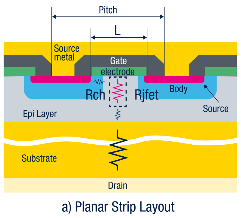
Opportunities to optimize planar power transistors, to reduce RDS(ON)
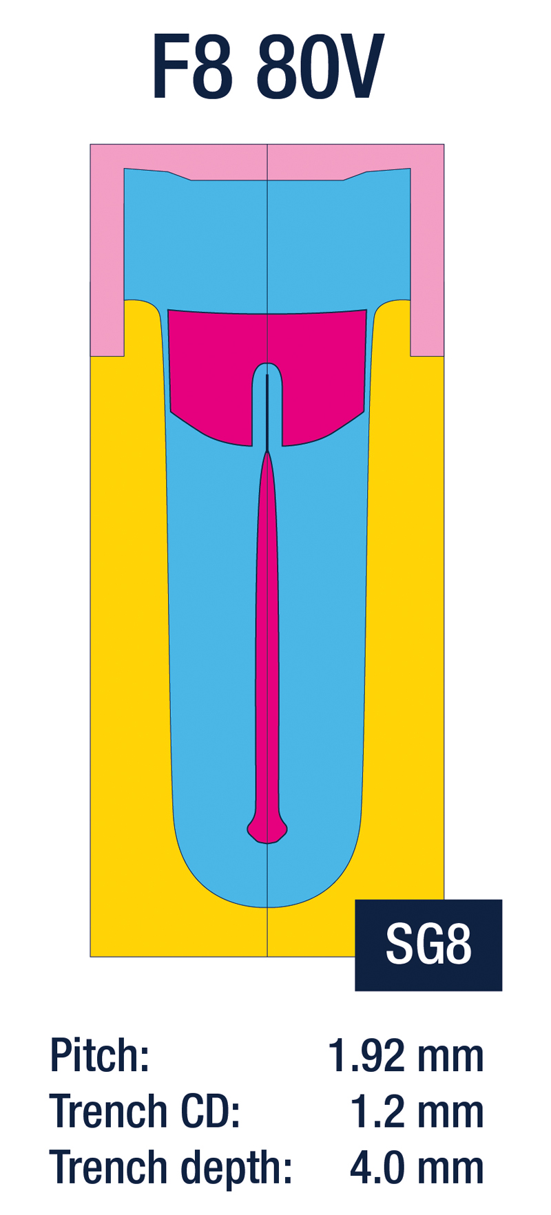
are limited due to the unavoidable additional channel resistance introduced by the parasitic JFET that forms between the body regions (figure 3a). In contrast, this JFET is not formed in the deep trench structure (figure 3b) of MOSFETs such as STPOWER’s 80/100V STripFET™ F7 and 100V STripFET™ F8.
Click image to enlarge
Figure 3a: Parasitic resistance between the body regions in planar MOSFETs
Click image to enlarge
Figure 3b: The deep trench structure has no parasitic resistance
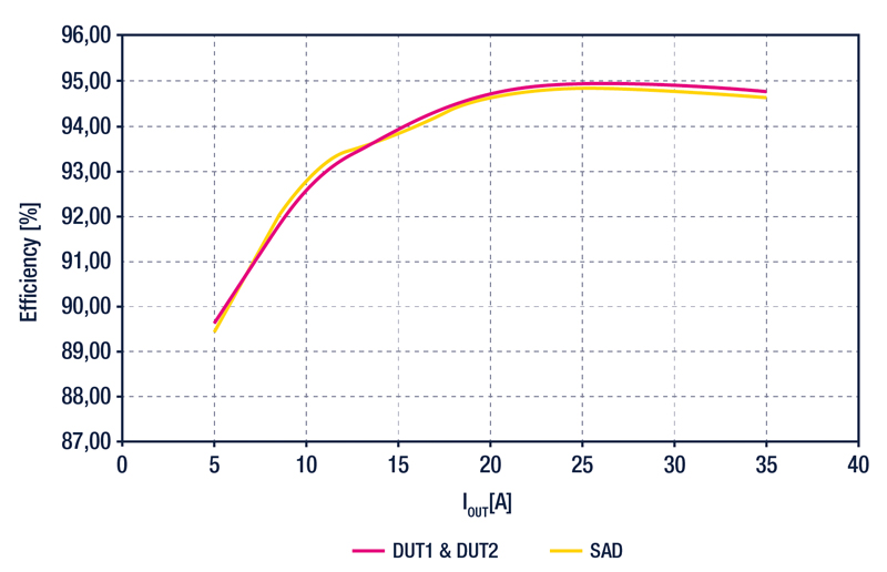
Figure 4 shows that the maximum efficiency of the LLC converter reaches close to 95% when deep trench synchronous MOSFETs are used in the secondary-side (DUT2) low-voltage circuit.
Click image to enlarge
Figure 4: PSU efficiency with deep trench MOSFETs in the low-voltage circuit
Conclusion
Key properties for AI-grade power supplies are established and require designers to enhance power handling, efficiency, and density. Wide-bandgap semiconductors are ideal. On the other hand, silicon superjunction transistors can offer competitive performance at lower costs and are continuously improving.
Superjunction and wide-bandgap technologies have capacitive hysteresis that complicates loss measurements in ZVS topologies. An accurate methodology for measuring the losses confirms that deep trench MOSFETs with low RDS(ON) low gate charge, and optimized parasitic capacitances, are suited for low-voltage synchronous rectification in the secondary side of tomorrow’s AI data-center power supplies.