A Look at GaN Technology Adoption Challenges in Power Electronics
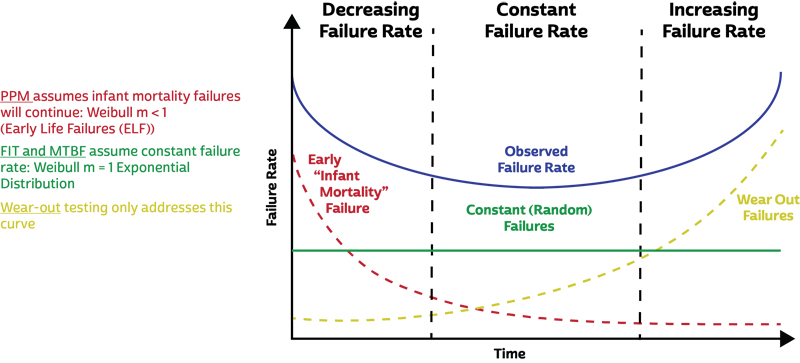
Figure 1: Reliability Bathtub Curve
2012 marked the long-awaited arrival of 600 V+ Gallium Nitride (GaN) transistors. Having already begun to make a mark in low-voltage applications, the wide-bandgap semiconductor material was expected to bring to high voltage (HV) power systems all of its inherent benefits: faster switching, higher power density, cooler thermal performance, and the ability to increase power efficiency at a lower overall system cost.
Yet, more than six years later, there is still some debate about HV GaN’s viability in in-production end products. And, perhaps, understandably so given the power electronics’ markets appropriately conservative approach to adopting technologies in early maturation stages.
What follows are common concerns often raised by end product manufacturers seeking to answer the fundamental questions: Is GaN right for my design? Is it ready?
Myth: Quality and Reliability Data is Unavailable or Not Good
Customer confidence begins with a GaN platform’s Quality and Reliability (Q+R). Given that HV GaN is in the early stages of adoption, understandably—the majority of data available is Intrinsic Lifetime or Wear-out data generated by the semiconductor manufacturers themselves.
And, industry qualification standards such as JEDEC (semiconductor industry) and AEC-Q101 (automotive industry) have not yet fully ratified GaN-specific testing. Available qualification test methodologies are designed for Silicon [Si]. So, while JEDEC and AEC-Q101 qualifications are important indicators of a GaN platform’s Q+R, customers vetting GaN should expect extended JEDEC tests that stress the thresholds of the GaN platform beyond the limits set for Si.
Yet, agreed, the above alone do not paint a full picture. More validation testing is needed. And, contrary to popular belief, it is available.
650 V GaN devices are in production and in use by customers shipping products today. As a result, Extrinsic Lifetime or Early Lifetime Failure [ELF] data and Field Failure rates are available from manufacturers such as Transphorm. This data [reported in Failure in Time or FIT and Parts per Million or ppm rates] is used by companies to understand infant mortality rates and to calculate end product warranty risks and costs. On a whole, it’s important for customers to understand the three sections of the reliability bathtub curve [Figure 1] and make sure their supplier can support all regions with data and background information in order to help them make sound decisions for application designs.
And, initial reports are positive showing ELF rates of .45 FIT and 4 ppm along with Field Failure rates of 3.1 FIT and a conservative estimate of 27.4 ppm. Notably, the current GaN Field Failure rate of 3.1 FIT is in line with the more mature Silicon Carbide [SiC] technology’s reported FIT rate of less than 5 FIT. [For baseline context, the lower the FIT and ppm rate, the more reliability the technology.]
Myth: E-mode Devices are Better than Two-chip Normally-off GaN FETs
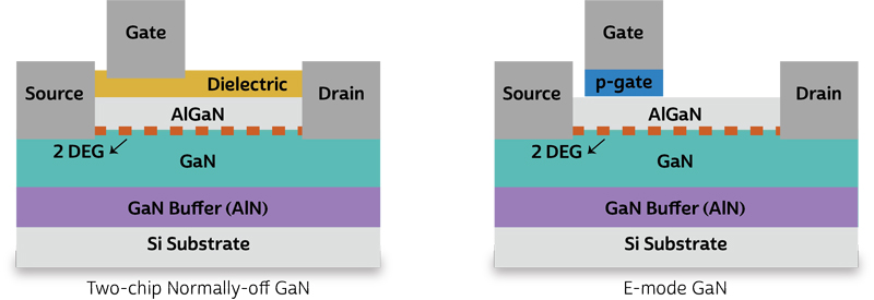
Today, the HV GaN power conversion industry is marketing two device “flavors”: enhancement-mode [e-mode] and two-chip normally-off GaN FET indicated in Figure 2. Misconceptions exist that suggest only e-mode devices are viable and practical in designs, leading to confusion over which flavor is the right one for a particular product. Here is where end product manufacturers need to take a moment and assess the value propositions offered by GaN and re-evaluate those within the context of these differing transistor types.
Click image to enlarge
Figure 2: Device structure of two chip normally-off GaN FET GaN devices versus e-mode GaN devices
A known advantage of GaN is its ability to switch faster than traditional Si, but also to remove a loss-causing component, particularly the bridge rectifier in a bridgeless totem-pole power factor correction configuration. This generally leads to higher efficiency resulting in a smaller system size and overall system cost reduction.
Yes, e-mode is a single-chip normally-off device. However, e-mode GaN transistors require many passive components and, sometimes, active (i.e. MOSFETs) devices to function properly in all operating modes. The additional supporting gate and start-up circuitry required to drive e-mode devices can increase chances of failure and is counter-intuitive to the configuration’s perceived simplicity.
Comparatively, two-chip normally-off GaN FETs do not have the same requirements. External component counts are low and the FETs can be paired with off-the-shelf drivers—for example—keeping complexity and related costs to a minimum.
It’s also important to note that many e-mode devices today are available only in surface mount packages. Inarguably, these packages have their place. But, as power levels increase, they can produce new design and thermal dissipation issues—requiring them to be paralleled which increases cost both in devices and printed circuit board [PCB] real-estate. These issues can sometimes cause problems when qualifying power supply units for high volume manufacturability and should be considered when determining the type of GaN devices to use.
Alternatively, two-chip normally-off GaN FET devices are available in standard 3-leaded TO-XXX packages. TO-XXX devices are well-known in the market having been used for many decades; are easy to mount and heatsink; and allow single devices to be used in applications reaching the several kW level.
Myth: Design Challenges are Too Limiting
High voltage GaN FETs are not the same as Si transistors when it comes to the physical structure. Silicon FETs are vertical whereas GaN FETs are lateral. Additionally, GaN devices can switch faster and operate at frequencies in the MHz (already available as RF devices). And, for many end product manufacturers, a digitally controlled AC to DC topology such as the bridgeless totem-pole PFC is where GaN offers its highest value.
So, yes, there may be a learning curve here. Initially. But, keep in a mind a few things.
First, HV GaN manufacturers, are releasing reference designs, app notes, white papers, training videos, and more to help close the knowledge gap. Further, manufacturers like Transphorm—a company currently producing third generation GaN FETs—are steadily modifying the GaN platform to reduce design complexity based on customer design and field experiences. In short, the technology continues to get better—we’re only in the early stages of innovation.
Second, companies like Telcodium have previewed complete power system modules to speed GaN product development. Other partnerships continue to emerge with complementary technology companies that help remove related development challenges.
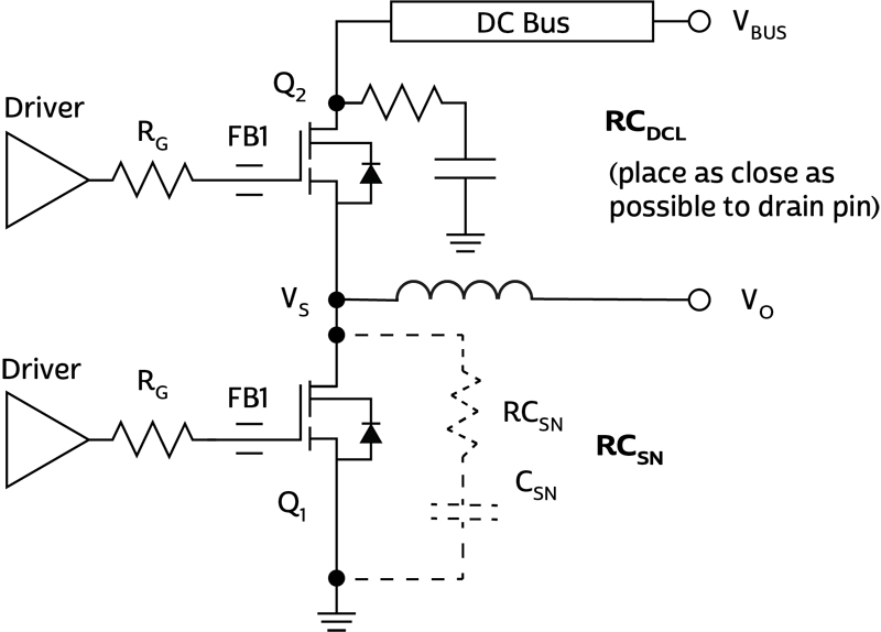
Third, misconceptions exist that design considerations such as electromagnetic interference [EMI] and slew control are suboptimal. High voltage GaN does have higher electron mobility [~1.5x that of Si]. Therefore, switching transitions and rise times are faster. So, particular attention must be paid to the PCB layout to manage noise. However, PCB design guides are available that are proven effective and provide a solid foundation to kick-start development. [See Figure 3.]
Click image to enlarge
Figure 3: Half-bridge switching circuit with GaN FETs demonstrates one approach to minimizing EMI
Related, slew rate control balances a switch’s performance to its EMI level. Despite the popular stereotype, slew rate control is achievable with all GaN technology versions. For example, it has been shown that two-chip normally-off GaN FETs can achieve a HV Si MOSFET-like speed both in di/dt (A/ns) and dv/dt (V/ns).
Fourth, misconceptions also exist that safety margins for GaN product development is unforgiving at an estimated low ≤ 1.7 V threshold and 1 V to 3 V maximum headroom gate robustness level. Two-chip normally-off GaN FET FETs are proven to deliver a larger threshold voltage of 4 V and a ± 20 maximum gate specification robustness as a decades-old Q+R low-voltage MOSFET is providing all the control—reducing the system’s overall sensitivity and giving design engineers a larger safety environment to operate within.
Myth: GaN FETs are Too Expensive
Today, high-voltage GaN is proven effective in power systems in the > 1.5 kW range, and is working its way down to the lower power levels as the technology evolves and prices reduce. In-production end products indicate notable power efficiency, performance, and power density increases; system size reductions; better thermal management; and more.
Yet, it needs to be a cost-effective solution compared to Si to fully compete across all potential application markets—particularly those where volumes are large such adapters. And, in a head-to-head comparison, GaN device costs today struggle to win when compared to those of Si transistors. However, the bigger picture needs to be considered.
Silicon offers a great cost-to-performance ratio. No argument. Unless the customer’s desired value proposition indicates otherwise, this makes GaN drop-in replacements unattractive and impractical in lower power applications such as traditional analog-controlled systems at < 1.5 kW.
As GaN pricing reduces over the next few years though, it will become more viable in that lower power range. Particularly when used with more well-known topologies such as standard PFC continuous-conduction mode [CCM] boost or other popular single ended circuits. [Transphorm estimates that year-over-year GaN platform innovation can lead to a price reduction of over 40% by 2020.]
Recapping the above, HV GaN power conversion technology is only in its early stages of maturation, leaving much room for innovation and optimization in the years and decades to come. Design challenges are being solved every day. Products are shipping today that outperform their predecessors. Major power semiconductor companies such as Infineon have stepped into the market. Complete validation data—including field failure rates—are now available and positive. Don’t fall for the challenge myths. Those facts are all testament to the simple reality that high voltage GaN has arrived and has a very bright future.
Transphorm

.jpg)