Author:
Molly Zhu, Analog Devices
Date
03/01/2021
 PDF
PDF
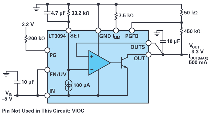
Click image to enlarge
Figure 1. −3.3 V output low noise solution
Low dropout (LDO) linear regulators have been widely used in noise-sensitive applications for decades. Nevertheless, noise requirements have become tougher to meet as the latest precision sensors, high-speed and high-resolution data converters (ADCs and DACs), and frequency synthesizers (PLLs/VCOs) challenge conventional LDO regulators to produce ultra-low output noise and ultra high power supply ripple rejection (PSRR). For instance, when powering a sensor, the supply noise directly affects the measurement result accuracy. In addition, switching regulators are often used in power distribution systems to achieve higher overall system efficiency. To build a quiet power supply, an LDO regulator usually post-regulates the output of a relatively noisy switching converter without using bulky output filtering capacitors. The high frequency PSRR performance of the LDO regulator becomes the predominant feature.
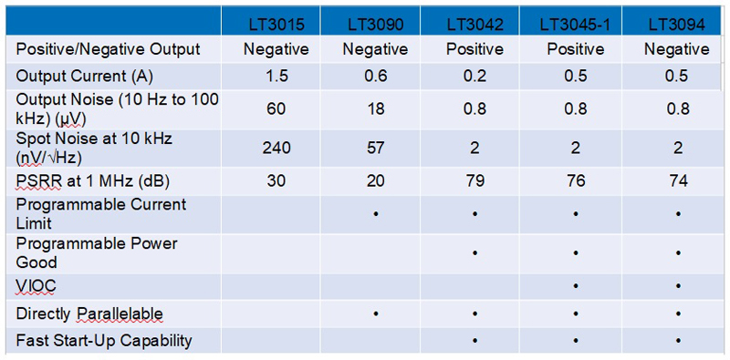
The LT3042, introduced in 2015, is the industry’s first linear regulator with only 0.8 µV rms output noise and 79 dB PSRR at 1 MHz. Two similar devices, the LT3045 and LT3045-1, increased the current rating and added features. All of these devices are positive LDO regulators. When a system has bipolar instruments, such as op amps or ADCs, a negative LDO regulator must be used in a polarity power supply design. LT3094 is the first negative LDO regulator that has ultralow output noise and ultrahigh PSRR. Table 1 lists the main features of the LT3094 and related devices.
Typical application
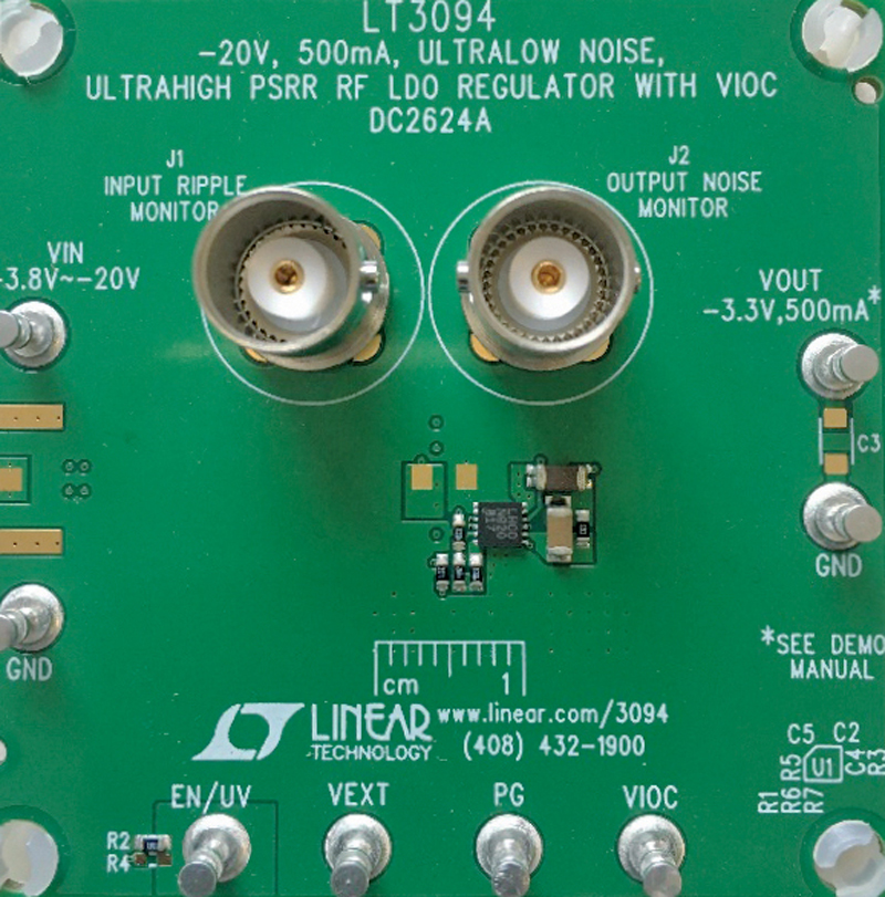
The LT3094 features a precision current source reference followed by a high performance output buffer. The negative output voltage is set with a −100 µA precision current source flowing through a single resistor. This current reference-based architecture offers a wide output voltage range (0Vto−19.5V) and provides virtually constant output noise, PSRR, and load regulation independent of the programmed output voltage. Figure 1 shows a typical application and the demonstration board is shown in Figure 2. The overall solution size is only about 10 mm × 10 mm.
Click image to enlarge
Figure 2. Demo circuit shows a tiny −3.3 V solution
Click image to enlarge
Table 1. Features of the LT3094 and Low Noise LDO Regulators
The LT3094 has ultra low output noise, 0.8µV rms from 10Hz to 100kHz, and ultra high PSRR, 74 dB at 1 MHz. Moreover, the LT3094 has programmable current limit, programmable power good threshold, fast start-up capability, and programmable input-to-output voltage control (VIOC). When the LT3094 post regulates a switching converter, the voltage across the LDO regulator remains constant by the VIOC function if the LDO regulator’s output voltage is variable.
The LT3094 avoids damage through internal protection, including internal current limit with foldback, thermal limit, reverse current, and reverse voltage.
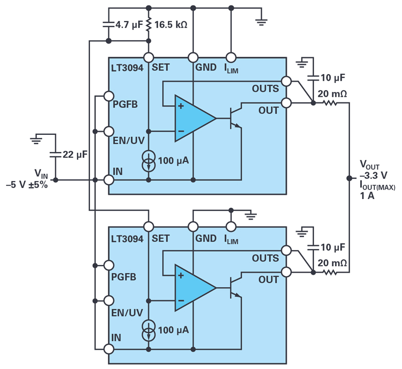
Direct paralleling for higher current
The LT3094 can be easily paralleled to increase output current. Figure 3 shows a solution using two LT3094s paralleled to achieve 1A output current. To parallel two devices, the SET pins are tied together, and one SET resistor, RSET, is placed between SET pin and ground. The current flowing though RSET, is 200µA, twice the amount of the SET current in one device. For good current sharing, a small 20mΩ ballast resistor is used at each output of the LT3094.
Click image to enlarge
Figure 3. Schematic of two paralleled LT3094s
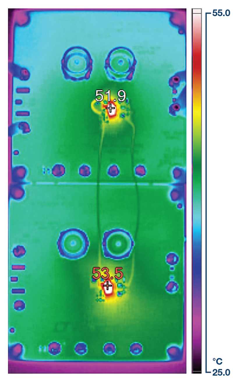
Figure 4 shows the thermal performance of the circuit in Figure 3 with−5 V input voltage and −3.3 V output voltage running at 1 A load current. The temperature of each part rises to about 50°C, indicating the heat is distributed equally. There is no limit on the number of devices that can be paralleled for even high output current and low output noise.
Click image to enlarge
Figure 4. Thermal image of two paralleled LT3094s
Dual positive and negative power supplywith variable output voltages
A power supply is generally built with a switching converter postregulated by an LDO regulator to achieve low output noise and high system efficiency. The optimized voltage difference between the LDO regulators input and output is about −1 V in order to maintain a good trade-off between power dissipation and PSRR. Maintaining this voltage difference is complicated in a variable output voltage system, but the LT3094 includes a tracking feature, VIOC, which keeps the voltage across the LDO regulator constant even as the output voltage varies.
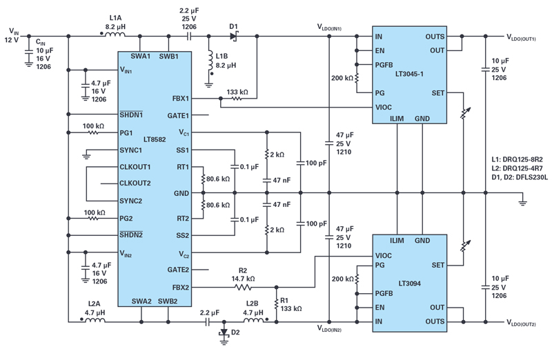
Click image to enlarge
Figure 5. Adjustable dual output, positive/negative power supply features high ripple rejection and cool operation
Figure 5 is the schematic of a dual power supply using LT8582, LT3045-1, and LT3094. The LT8582 is a dual-channel PWM dc-to-dc converter with internal switches that can generate both positive and negative outputs from a single input. The first channel of LT8582 is configured as a SEPIC to generate a positive output, and the second channel is an inverting converter to generate the negative rail. In the negative rail, the voltage across the LT3094 is controlled by VIOC voltage as
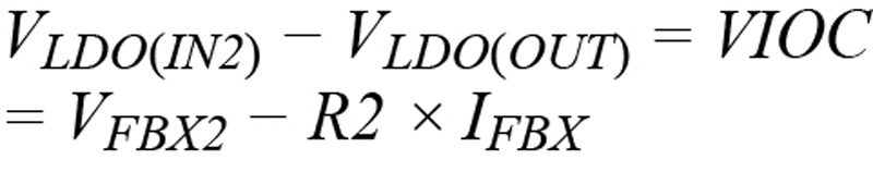
where VFBX2 is 7 mV and IFBX is 83.3 µA. Setting R2 to 14.7 kΩ sets the VIOC voltage at –1.22 V over the variable output voltage. The resistor R1, at 133kΩ, limits the input voltage of LT3094 to –16.3V, calculated by

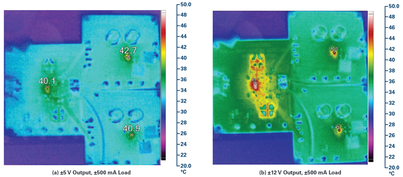
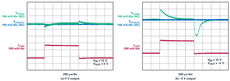
The thermal images of the circuit running at 12V input are shown in Figure 6. When output voltage changes from ±3.3 V to ±12 V, the temperature rise of the LT3094 remains constant. Table 2 lists the voltage and current of all three devices. Figure 7 shows the transient response of the ±5 V power supply running at 12 V input.
Click image to enlarge
Figure 6. Thermal image of a dual power supply at 12 V input

Click image to enlarge
Table 2. Circuit Performance of Dual Output Positive/ Negative Power Supply at 12 V Input, ±500 mA Loa
Click image to enlarge
Figure 7. Transient response of dual power supply at 12 V input, ±5 V output
In Figure 5, no additional capacitor other than the output capacitors at LT8582 is placed at the input of the LT3094. Generally, an input capacitor reduces the output ripple, but this is not the case for the LT3094. If the LT3094 has input capacitors, the switching currents from the switching converter will flow through the input capacitor, causing the electromagnetic coupling from the switching converter to the LT3094’s output. The output noise will be increased, degrading the PSRR. Provided that the switching regulator is placed within two inches of the LT3094, we recommend not placing a capacitor at LT3094’s input to achieve best PSRR performance.
Conclusion
The LT3094 is a negative LDO regulator featuring ultra low noise and ultra high PSRR. It features a current reference-based architecture that keeps noise and PSRR performance independent of the output voltage, and enables multiple LT3094s to be easily paralleled for increased load current and reduced output noise. The VIOC function minimizes the power dissipation of the LDO regulator when the LT3094 post regulates a switching converter, making it ideal in variable output voltage applications.