New Ultralow Quiescent Current Buck-Boost Converters Power Industrial Systems & More

Buck-boost DC/DC converter is one of the most valuable tools in a power supply designer’s toolbox
A buck-boost DC/DC converter is one of the most valuable tools in a power supply designer’s toolbox for dealing with a variety of power conversion scenarios. In these situations, input voltages can vary widely due to non-ideal or multi-input power sources, transient disturbances or charging and discharging storage elements. Single inductor, non-inverting buck-boost converters seamlessly step-down (buck) or step-up (boost) an input voltage and regulate the output voltage, regardless of whether the input is above, equal to or below the output. The buck-boost converter’s three-way flexibility can replace two ICs (a separate buck converter or a low-dropout linear regulator, plus a boost converter), thus saving space/footprint on the printed circuit board (PCB) and simplifying the bill of materials (BOM). These converters greatly enhance battery life in portable systems as they take advantage of more of the battery’s useful input voltage range while regulating the output. In the case of multiple potential power sources, a buck-boost converter can be used in exclusively buck or boost mode, depending on the power source. Further, in a power backup application, where a discharging storage element has a discharge voltage curve that spans the required fixed output, a buck-boost converter will exercise both modes of operation.
Application Conditions Vary by Market Segment
Other than consumer products, input and output voltage ranges can vary widely depending on the application. For instance, in automotive environments, the 12V car battery is the main supply for all electronics. However, that nominal 12V can dip to as low as 3V during cold cranking or spike up to near 40V (limited by a transorb) during a load dump condition. In industrial applications, standard power bus voltages are either 24V or 12V; in addition, higher voltage power supply spikes with durations ranging from a few microseconds to hundreds of milliseconds are commonly encountered. The electronics in these systems must not only survive transient voltage spikes, but in many cases also operate reliably throughout the event. Industrial and military/aerospace systems require wide operating temperature ranges and robust power delivery to essential downstream electronics, even under stringent input voltage conditions (just like the automotive environment). Further, avionics, military and aerospace environments have standard power rails, but can also operate from various battery configurations and solar panels, thus requiring power supplies that can handle a very wide input voltage range. Some applications need to accept many different input sources, so that any energy source will automatically power the system. Many military applications, for example, must accept different types of batteries, adapters and even solar panels to provide their power.
Since these systems require multiple well-regulated power rails, the lower voltage rails are typically supplied by buck regulators or LDOs. There are requirements however, for stabilized medium-to-high level 12V and 24V rails for powering sensors and various analog functions (op amps, motors, or transceivers). Many of these require both buck and boost conversion, depending on the power bus voltage level or the system configuration. A buck-boost converter (in some cases with solar capability) provides the flexibility to regulate the output from a variety of input sources, minimizing the number of power converters in the design and thus simplifying the BOM.
Power Conversion Design Challenges
In the past, designs requiring both buck and boost mode operation have been solved by using multiple power converters with their typical issues of PCB area, size, higher cost, greater complexity, lower reliability, higher quiescent current (IQ) and lower conversion efficiencies. An alternative topology such as SEPIC (single-ended primary inductance converter), while simpler than multiple power converters, is about 10% lower efficiency than a synchronous buck-boost converter and requires two inductors and a high current coupling capacitor, adding complexity and potential noise, as well as reduced battery life.
Boost mode operation in a buck-boost converter presents its own set of unique challenges, particularly when the boost converter is turned off, or during initial application of the power source. The conventional boost converter has a direct path for current from VIN to VOUT through the inductor and the boost diode. This unfortunate aspect of the boost converter can cause a large and potentially damaging inrush current when power is applied to VIN and thus keeps VOUT partially powered, with a diode drop below VIN when the power converter is shut down. Fortunately, many of Linear Technology’s buck-boost converters feature an output disconnect feature that is inherent in their 4-switch architecture. Thus, on initial application of power to VIN, the buck-boost converter’s input current is kept under control, gradually ramping from zero up to the current limit level while VOUT powers up. When turned off, the buck-boost converter completely disconnects VOUT from VIN, so that VOUT can safely discharge all the way to zero.
Newer but maturing Li-Ion Phosphate battery chemistries enable longer run times, but their voltage discharge profiles are extended, with significant energy available at battery voltages below 3V. This characteristic influences the related power conversion system, making synchronous buck-boost regulators necessary to generate outputs of 3V or above, common in many systems including industrial.
Some backup applications that use supercapacitors are better served with buck-boost converters that can run down to very low input voltages. For example, a bank of capacitors (supercapacitors, electrolytics, etc) gets charged to some voltage level. Should the power fail, the downstream buck-boost converter can maintain output regulation since it has the benefit of allowing the use of all the energy in the capacitors. This can reduce the amount of capacitance needed in the application (reducing the capacitance and board area). However, a more modern converter still needs 2.xV of input voltage to operate. Users therefore need to play some tricks (backfeeding, etc.) if they want to pull power from an input which is less than 2.xV. Many DC/DC converters cannot do this.
Fortunately, Analog Device’s buck-boost converter products solve many of these issues. For inputs requiring 40V capability, the LTC3115-1/-2 and LTC3114-1 are well-suited. For input voltage up to 15V, the LTC3111, LTC3112 and the ultralow quiescent current LTC3129 are available. A near term future LTC311x family product will extend input voltage capability to 18V and support 5A of output current in buck mode. Nevertheless, there has been a gap in the industry that has not been addressed – a buck-boost DC/DC converter compatible with 12V/24V systems, which also has moderate output current up to 600mA, low-voltage operation after start-up and ultralow quiescent current.
New Ultralow IQ Buck-Boost Converters
It is clear that a buck-boost solution that solves the issues described should have the following attributes:
• Operation over a wide input/output voltage range
• Sufficient output current capability
• Ultralow IQ
• Low output noise/ripple
• High efficiency operation
• Output disconnect when operating in boost mode
• Minimal external components required, easy to design
• Excellent thermal performance
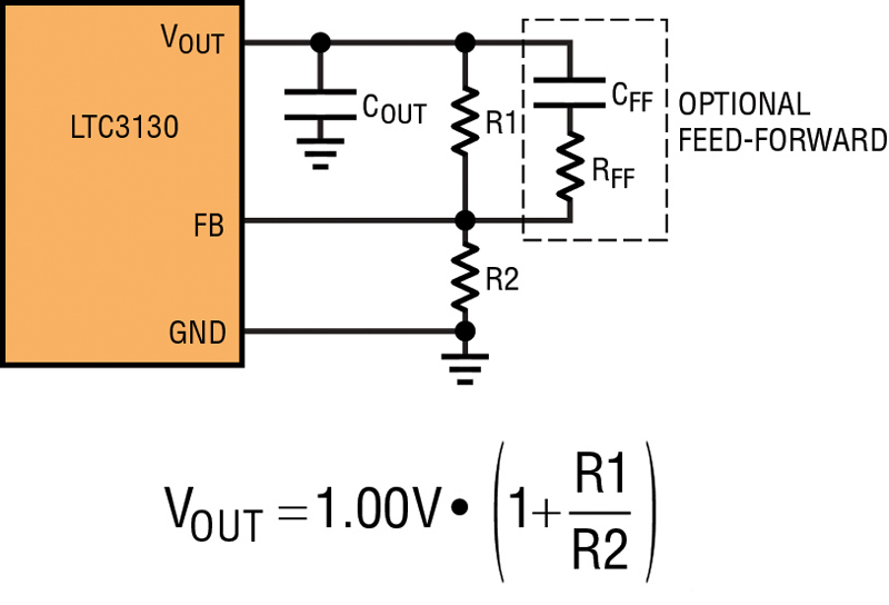
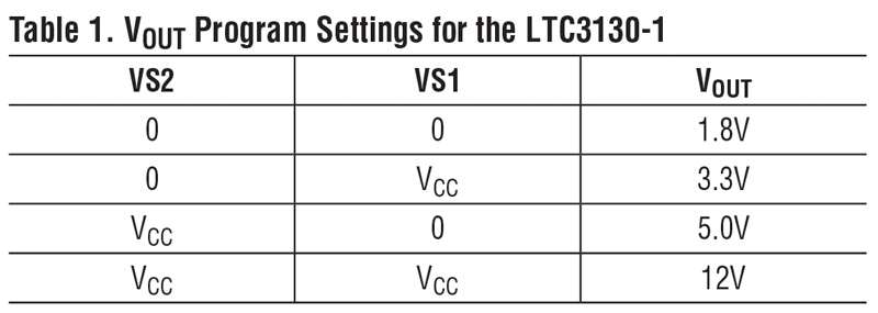
To address these needs, Analog Devices recently introduced the LTC3130 and LTC3130-1. These 25V input and output rated monolithic synchronous buck-boost converters can supply up to 600mA of output current in buck mode, and have an extremely low 1.2µA no-load quiescent current (see Figure 1). Each device offers 2.4V to 25V input voltage range and 1V to 25V output range (LTC3130 is adjustable, see Figure 2) and provides a regulated output with inputs above, below or equal to the output. Once started, the devices have only a 0.6V typical input voltage requirement. User-selectable Burst Mode operation lowers quiescent current to only 1.2µA, improving light load efficiency and extending battery run time. The proprietary buck-boost topology of the LTC3130/-1 provides low noise, jitter-free switching through all operating modes, ideal for RF and precision analog applications that are sensitive to power supply noise. The devices also include programmable maximum power point control (MPPC) capability, ensuring maximum power delivery from non-ideal power sources such as photovoltaic cells. The LTC3130-1 shares all of the features of the LTC3130, but offers four user-selectable fixed output voltages: 1.8V, 3.3V, 5V and 12V, eliminating the resistor divider required for the adjustable output version (See Table 1).
Click image to enlarge
Figure 2. VOUT Feedback Divider Equation and Schematic for the LTC3130
The LTC3130/-1 have sufficient voltage margin to handle 1-6 series lithium battery input systems and nominal 12V systems subject to large noise spikes, as well as the ability to power 24V sensors. A guaranteed minimum 660mA inductor current limit provides boost mode output current capability, particularly for 24V sensors that must operate from low input voltages, such as 3.3V or 5V or batteries.
Table 1. VOUT Program Settings for the LTC3130-1
Click image to enlarge
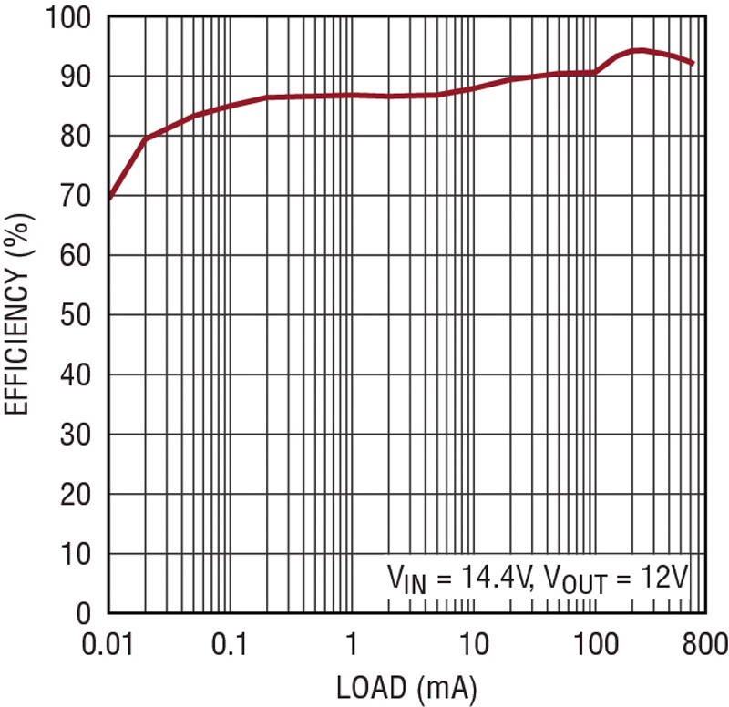
The LTC3130/-1 includes four internal low RDSON N-channel MOSFETs to deliver efficiencies of up to 95%. Converter start-up can be achieved from sources capable of supplying as little as 7.5µW, making the LTC3130/3130-1 ideal for applications powered by weak sources, including thin film solar cells. Alternatively, Burst Mode operation can be disabled, offering low noise continuous switching. The LTC3130/-1’s constant 1.2MHz switching frequency ensures low noise and high efficiency, while minimizing the size of the external components (see Figure 3).
Click image to enlarge
Figure 3. LTC3130/-1 Efficiency is 94% for 14.4VIN to 12VOUT at 200mA
Built-in loop compensation and soft-start reduce external parts count and simplify design. Other features include a power good indicator, pin-selectable current limit, an accurate RUN pin threshold, an external VCC input and thermal shutdown. The device’s combination of tiny externals, wide operating voltage range, compact packaging, plus ultralow quiescent current makes the LTC3130/-1 well suited for always-on applications in which extended battery run time is of primary importance. Applications include long life battery-powered instruments, portable military radios, low power sensors and solar panel post-regulator/charger circuits.
Integrated into the LTC3130/-1 are 2 low dropout (LDO) regulators to generate VCC–one from VIN and one from EXTVCC. So long as sufficient voltage is maintained on VCC, the converter will work from any input source.
The LTC3130/-1 is available in thermally enhanced 20-lead 3mm x 4mm QFN and 16-lead MSOP packages. E- and I-grade devices are specified over the –40°C to 125°C operating temperature range.
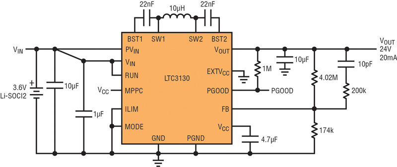
24V Sensor Application
Figure 4 highlights a battery-powered 24V sensor power supply. Power for the sensor is provided by a high reliability, long life, lithium thionyl chloride primary battery. To maximize service life, the sensor is only activated for brief intervals with a long time period between activations, reverting to a near zero power state when inactive. The 200mA input current limit option of the LTC3130 is used (Ilim pin=GND) to minimize peak currents taken from the high output impedance primary lithium thionyl chloride battery when the sensor is activated, further prolonging the service life of the battery. The LTC3130 is shut down by driving its RUN pin low during long idle periods, drawing only 1µA from the 24V output. The sensor is also disconnected from the 24V rail, or shut down to minimize discharge of the 24V output capacitor during the long idle periods. With the 24V output maintained in this fashion, the sensor can power up quickly, make the required measurement then power down again, without having to wait for the 24V power rail to charge. During normal operation of the sensor this DC/DC converter achieves up to 83% efficiency.
Click image to enlarge
Figure 4. Battery-Powered 24V Converter with 200mA ILIM to Limit Battery Droop
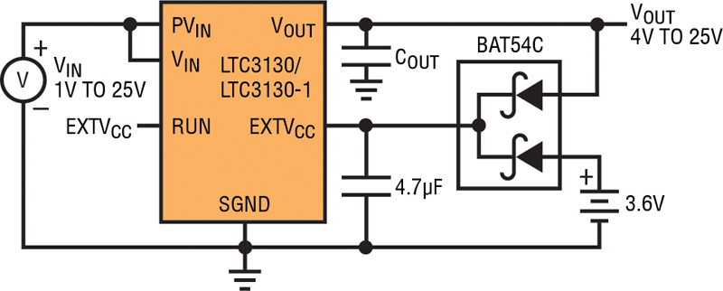
EXTVcc Capability
The LTC3130’s EXTVCC powers the IC if >3V (range: 3V to 25V). The EXTVcc input can be used for:
- Bootstrapping to VOUT to allow lower VIN capability
- Bootstrapping to VOUT for improved efficiency at high VIN
- Start-up from an external source for very low VIN applications (see Figure 5)
Click image to enlarge
Figure 5. LTC3130/-1 Converter Bootstrapped to VOUT to Eliminate Battery Drain while Allowing Start-up and Regulation with a VIN Source of 1V or Less
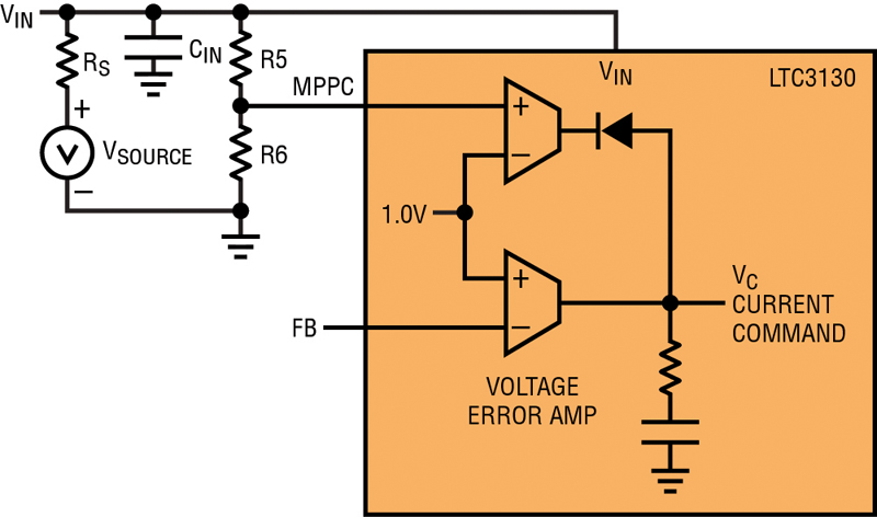
Maximum Power Point Control
The maximum power point control (MPPC) input of the LTC3130/-1 can be used with an optional external voltage divider to dynamically adjust the commanded inductor current to maintain a minimum input voltage when using high resistance sources, such as photovoltaic panels, to maximize input power transfer and prevent VINfrom dropping too low under load. The MPPC circuit servos the input voltage of the converter to a programmable point for maximum power extraction when operating from various non-ideal power sources such as photovoltaic cells. Refer to Figure 6 for details.
Click image to enlarge
Figure 6. MPPC Amplifier with External Resistor Divider
Conclusion
The single inductor, noninverting buck-boost converter is an extremely flexible and valuable power supply component. Analog Device’s LTC3130/-1 are 25V input and output rated monolithic buck-boost converters with a 600mA output current rating in buck mode and an extremely low 1.2µA quiescent current. These devices extend the buck-boost application reach to encompass a wide variety of challenging power supply requirements, including loosely regulated 5V / 12V / 18V adapters, multiple battery types, small solar cells and rechargeable sources. Their flexibility and features such as MPPC and EXTVcc enable a range of unique powering scenarios that are ideally suited to solve problems across a wide variety of applications.
Analog Devices