IGBT Modules for vehicle inverter systems need high power density, low loss, and light weight
The automotive industry is under significant societal pressure to address global warming. Electric vehicles (EV) and hybrid electric vehicles (HEV) are expected to lead the way in CO2 reduction, relying on their internal inverter systems to control high electric power in the limited space available. Due to these space constraints, the IGBT Module used in the inverter system requires high power density, low loss, and light weight
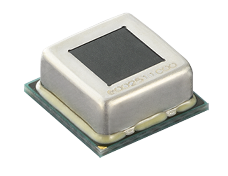
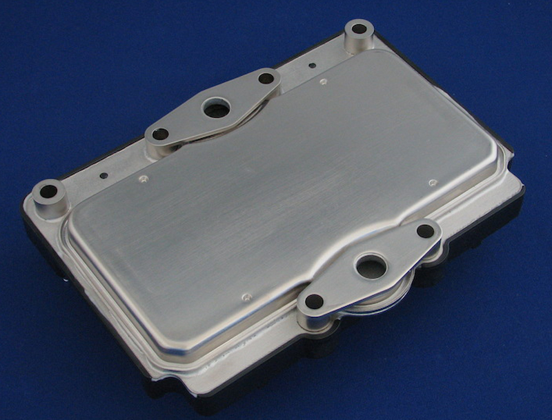
For example, Figure 1 shows the next-generation Fuji Electric standard IGBT module for EV and HEV systems, while Figure 2 displays the backside of the IGBT module. The aluminum water jacket has an optimized cooling flow structure inside that effectively transfers the generated heat to the cooling liquid. The flange structure with coolant inlet and outlet is embedded into the water jacket. This plug connection simplifies the link to the liquid cooling system and supports the specification of flow rate.

Click image to enlarge
Figure 1: next-gen Fuji standard IGBT module
Click image to enlarge
Figure 2: Backside of IGBT module
The applied IGBT and FWD chips reduce the module loss by using Fuji Electric’s seventh-generation chip technology and Reverse-Conductance IGBT technology, resulting in a reduction in the overall module dimension of the IGBT.
Designing cooler tech
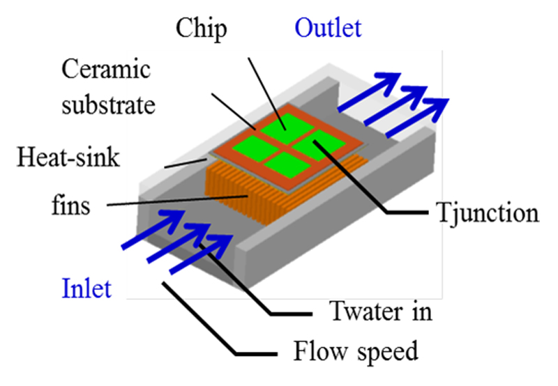
Typically, IGBT power modules with cooling fins and cooling systems must be designed by the inverter manufacturer separately and then tightened together using sealing material, so it is imperative that the manufacturer secures minor production tolerances. Fuji Electric was able to estimate the impact of the clearance on the heat radiation performance using a simplified model.
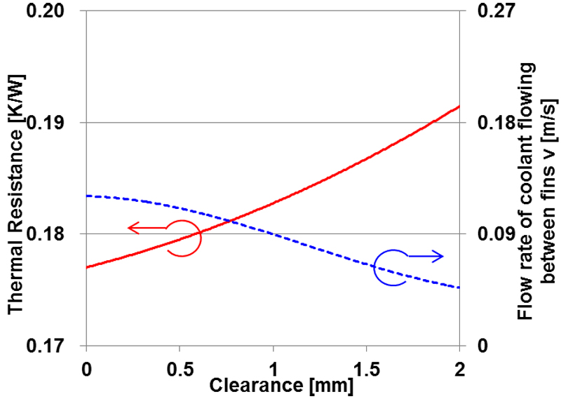
In this case, the fins have a thickness of 1mm and height of 10mm at intervals of 1 mm, and the coolant speed was set to flow evenly into the coolant inlet with 1 liter/min. Figure 3 a&b shows the simplified model and simulation results, and demonstrates that a larger clearance causes the thermal resistance to increase as the coolant flows to the area of lowest pressure resistance and spreads out in a wide clearance cross-sectional area, thereby reducing the flow rate between the fins.
Click image to enlarge
Figure 3a: Simplified model and simulation results
Click image to enlarge
Figure 3b: Simplified model and simulation results
In addition, parallel connection of the modules is estimated to cause a significant reduction in the coolant flow rate, by indicating that integration of the heat sink and water jacket leads to a beneficial effect of eliminating the clearance issue. Moreover, it is effective in increasing the coolant flow rate between fins and decreasing the thermal resistance.
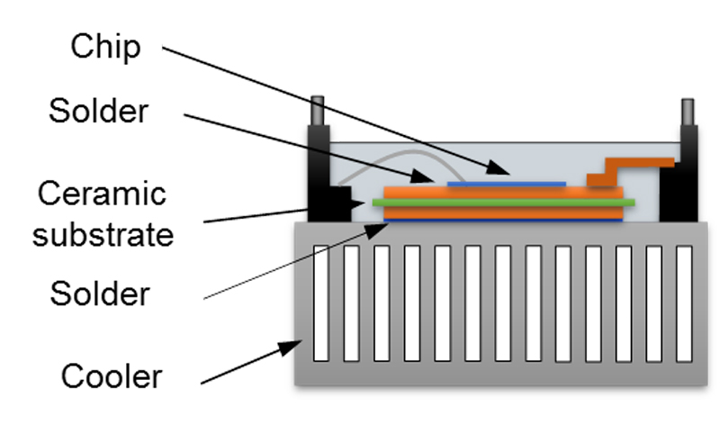
Figure 4 shows a cross-sectional view of the new module structure, where the aluminium direct liquid cooling structure has been applied for the new package. In the new structure, the water jacket and fin pins are fused to one unit to eliminate the clearance issues. This has resulted in a cooling structure, which maximizes the performance of the coolant. The ceramic substrate that belongs to the base plate has been made thinner and accessory high heat conductivity material was used.
Click image to enlarge
Figure 4: Cross-sectional structure of next-gen standard module
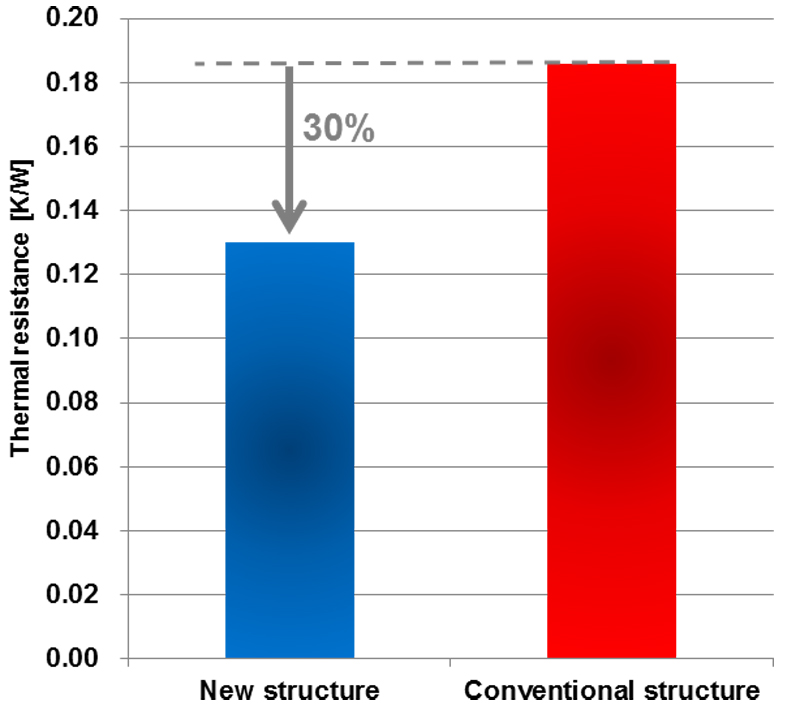
Figure 5 shows a comparison of the thermal resistance of conventional structures to the new structures. The New IGBT module structure combines the utilization of the coolant, high thermal conductivity and is capable of reducing the thermal resistance by 30% versus the conventional structure.
Click image to enlarge
Figure 5: A comparison of the thermal resistance of conventional structures to the new structures
Allowing continuous operation at 175°C
The heat generated in the chip during IGBT module operation is radiated from the cooling fins through the baseplate. The upper limit of junction temperature (Tj) is generally 150°C. Hence, the maximum operation temperature is determined by the temperature difference between the coolant temperature and the maximum junction temperature.
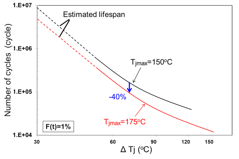
In order to maximize this temperature span it is possible to increase the junction operation temperature. Fuji Electric aimed to achieve higher output power by increasing the guaranteed upper limit Tjmax to 175°C and reducing the thermal resistance. In order to raise Tjmax from 150°C to 175°C, the impact of the element peripheral components on reliability must be improved. We used the conventional module structure to conduct a power cycle test with fixed Tjmax.
Figure 6 demonstrates the test results. A temperature rise of 25°C caused the lifespan to decrease by 40% at a ΔTj = 75°C.
Click image to enlarge
Figure 6: A temperature rise of 25°C caused the lifespan to decrease by 40% at a ΔTj = 75°C
Here, the focus on the lifespan decreases due to the solder bond under the element. With the conventional Sn-Ag-based solder, degradation due to thermal deterioration is a possible factor causing the lifespan to decrease. Fracture modes have been analyzed and a new solder material developed incorporating strengthening mechanisms to realize high thermal resistance and high strength.
Development of a reverse-conducting IGBT (RC-IGBT)
Fuji Electric is working on the development of 750V/800A class of an insulated-gate bipolar transistor (IGBT) module to be mounted in inverters for automotive applications. In order to meet the need for miniaturization as well as loss reduction of the in-vehicle module for improving fuel efficiency, a reverse-conducting IGBT (RC-IGBT) with a withstand voltage of 750 V was developed that integrates an IGBT and freewheeling diode (FWD) into one chip.
RC-IGBTs have already been commercialized as small-capacity chips for consumer electronics. However, as large-capacity chips required for in-vehicle use, technological hurdles for reducing loss have been too difficult to overcome up to now.
Heat radiation characteristics
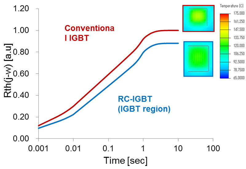
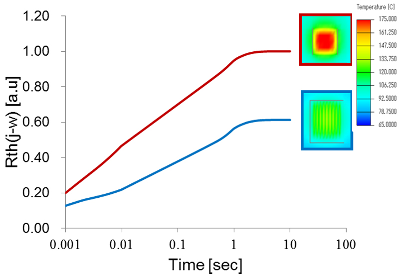
The RC-IGBT has achieved a reduction in the chip area and module dimension by integrating the IGBT and FWD. In addition, the RC-IGBT radiates heat from the FWD regions also via the IGBT regions, which makes the thermal resistance significantly lower than that of the conventional IGBT/FWD. A module with a direct liquid cooling structure has been used to compare the thermal resistance between the RC-IGBT and the conventional IGBT and FWD with the same active area (see Figure 7A&B). The thermal resistance of the IGBT regions of the RC-IGBT is 12% lower than that of the conventional IGBT and the thermal resistance of the FWD regions is 40% lower than the conventional FWD.
Click image to enlarge
Figure 7a&b: Thermal resistance based on same active area (a) RC-IGBT(IGBT-Region) and conventional IGBT (b) RC-IGBT(FWD region) and conventional FWD
Click image to enlarge
Figure 7a&b: Thermal resistance based on same active area (a) RC-IGBT(IGBT-Region) and conventional IGBT (b) RC-IGBT(FWD region) and conventional FWD
Effect to applications by module
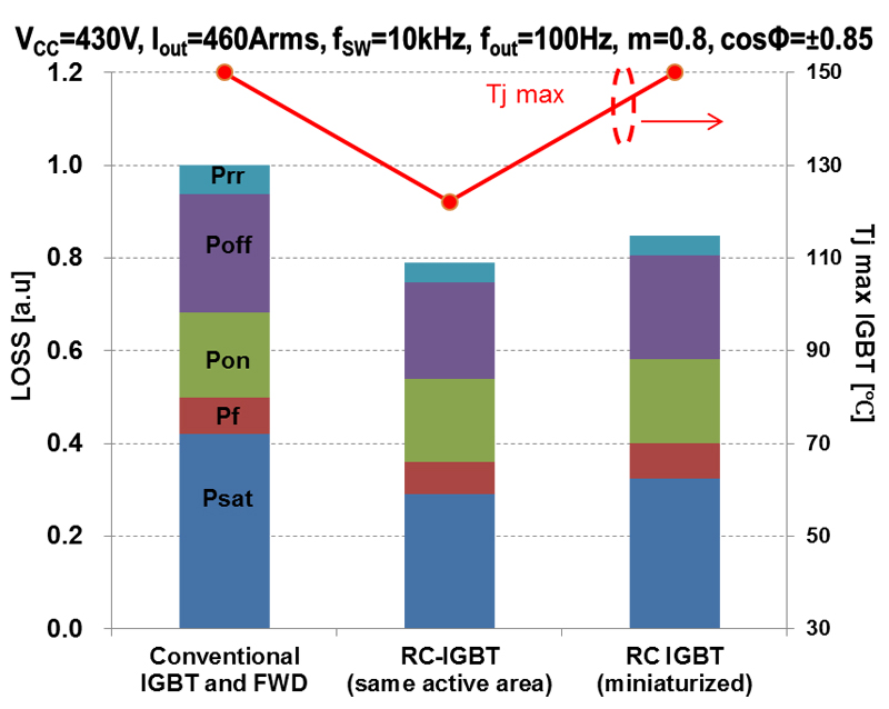
This section describes the miniaturization effect of the RC-IGBT as it is applied to the IGBT module for automotive applications. Figure 8 shows the results of calculating loss and temperature during inverter operation with the RC-IGBT having the same active area as the conventional IGBT and FWD and miniaturized RC-IGBT.
Click image to enlarge
Figure 8: Loss comparison between RC-IGBT and conventional IGBT&FWD
Table 1 shows a comparison of the chip active area and module area. As compared with the conventional IGBT, the RC-IGBT is capable of reducing power loss during inverter operation by 20% or more by reducing the saturation voltage, forward voltage and turn-off loss.

Click image to enlarge
Table 1: Chip active area and module footprint
In addition to reduce loss, the advantage of heat radiation described in section 5.4 allows the chip's maximum temperature to be lowered by about 28°C. The chip size of a module depends on the maximum temperature in operation. This result indicates that the RC-IGBT with smaller chip size can operate at the same level as an inverter of the same rating.
The RC-IGBT with the reduced size by 30% shows a temperature equivalent to the conventional IGBT and FWD, which means that the module area can be reduced by 15% for the same power rating.
Looking forward
Fuji Electric’s new standard IGBT module was developed to realize high power density by combining small-size and low weight to meet the demands for HEV/EV. As a result of the technological developments applied to the new standard module, three conclusions are reached:
1. A cooling design without clearance increases coolant flow speed between fins. This decreases thermal resistance due to the improvement of heat transfer efficiency. The thermal resistance is decreased by 30%.
2. High temperature operating technology was developed which allows for a continuous operation of 175°C. The power cycle lifetime is more than doubled when compared with the conventional products in all temperature ranges
3. An RC-IGBT integrating the IGBT and FWD into one chip was developed to realize loss reduction and downsizing compared to the conventional IGBT and FWD combination. The chip size is downsized by 30% compared to the conventional IGBT and FWD combination. As a result, a reduction of 58% in weight and 12% in size was achieved compared to other 800A power modules in the market.