
Keep RDS(on) low
With the recent upsurge in hybrid vehicle adoption and almost all major car OEMs now working on full electric vehicle projects, people often point out that this is old news. In many respects they are correct; the origins of the electric car can be traced back to the 1830s and by the late 1890s fleets of electric taxi cabs were running around the streets of several US cities. So what's different this time round? There have been two major barriers to the electrification of the car to date. The first is the dominance of the existing technology. In short the internal combustion engine is just too good. Modern engines are mass produced, cost effective, well understood, highly refined & reliable and supported by a universally established refueling and repair infrastructure. Now as governments scrutinize CO2 emissions, the internal combustion engine is coming under pressure from both ends with heavy taxes on the gasoline put into the tank and on the emissions flowing out of the exhaust. The second major obstacle to the electrification of the car is energy density. The main enablers here will be new battery technology and novel battery management schemes. But at the same time the systems which use the limited onboard supply of electrical energy will have to do so in a more intelligent way. An increasing awareness of efficiency is fueling a rapid change in the application landscape across all vehicle types. High power DC-DC converts, HID lighting, class D audio, electric power steering, 3 phase inverters and synchronous rectification will appear in increasing numbers on next generation cars, offering efficiency and good power density. Power MOSFETs will be a key enabling technology in both controlling the battery and its loads. By their nature power MOSFETs are not �ideal' switches. MOSFETs have a finite on-resistance, add parasitic parameters to the electrical path and, the more power needed the more space is required for switches and cooling assemblies. These all affect the power density and efficiency of a given power electronics system. How can this be improved? The power dissipation in the steady state of a semiconductor can be expressed as:
(1) Where Pd is the power dissipated in the semiconductor switch, Tj is the junction temperature, TA the ambient temperature of the surroundings and RthJA is the total thermal resistance from junction to ambient. Also considering the relationship between power, current and RDS(on)

(2) Combining 1 and 2 together we can link the current to the thermal resistances and the RDS(on):
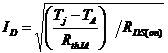
(3) This equation is important as it shows how the thermal management aspects of the design have a direct impact on the electrical performance of the system. Finally dividing by the area of the MOSFET's PCB footprint, AFP, we can arrive at the current density of the device.
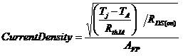
(4) On closer inspection of equation 4 the main obstacles to greater current density can seen. Minimize thermal resistance ? Maximize heat extraction The first step to increasing power density is to ensure that for a given RDS(on) the silicon in housed in a package which enables the heat generated to be easily extracted; RthJA must be as low as possible. To keep RthJA low semiconductor designers can increase the size of the silicon die, getting more die in contact with the package enables a better heat transfer to the outside world, a larger die archives this and has lower RDS(on), but at greatly increased cost. Alternatively the thermal resistances of the package can be reduced, perhaps with new materials or a new style of package. Most traditional power packages only have a single cooling path; through the bottom of the device to the PCB or heat sink. Great improvements can be made with the addition of a secondary cooling path; this is exactly what the DirectFET package enables via top side cooling.

Figure 1 compares and contrasts the thermal routes for getting the heat out of a Large Can DirectFET package and a D2Pak. In both cases the designer has attempted to achieve the lowest possible thermal resistance from junction to ambient by using both the downward thermal path from the junction to the PCB and the upward path through the package to a heat sink on top of the part. Both packages have good thermal resistance from the junction to the PCB with values of 0.5°C/W and 0.45°C/W for the Rth J-PCB of the DiretcFET and D2Pak respectively. By adding a second upwards thermal path these values can be reduced. The D2pak was not designed to be cooled through the top of its thick plastic package, but if this is attempted an Rth J-TOP (junction to top of package thermal resistance) of around 85°C/W will be seen compared to the DirectFET which has an considerably lower value of 1.2°C/W. When the overall thermal resistances of the two routes in parallel are compared the dual sided cooled DirectFET has a thermal resistance which is around half of the D2Pak. Using the second thermal route enables an instant improvement in the current density of the system.
Looking at the numerator of equation 4 after having kept RthJA low it's then important to consider the root cause of the heating - the on resistance of the device. A key figure of merit here is the semiconductor material and the design of the MOSFET itself. However silicon based MOSFET technology is maturing forcing manufacturers have to look to further afield to complex silicon solutions or new materials to keep the RDS(on) low. But it is also important to consider the effect of the package on the RDS(on) value or rather the limitations that the package places on delivering ultra low RDS(on) to the system. MOSFETs with an on resistance in the 1m? range at 40V are reasonably common in the market today and increasingly on such devices around half of the RDS(on) stated on the datasheet is attributed to the package. The resistance that the package adds to the silicon is know as the Die Free Package Resistance (DFPR) and figure 2 shows the DFPR values for various power packages.
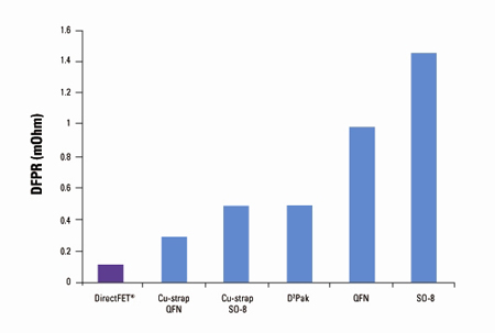
There is a large range in DFPR values between the existing plastic packages (shaded in green). Different wire bonding and lead frame options enable the DFPR to be greatly reduced to around 0.3m? in the case of the copper clip PQFN. However the lead frame and wire bonds on the traditional plastic packages still leave a relatively long electrical path between PCB and die. As the market continues to demand more efficient systems, at higher power levels, RDS(on) values will hit a fundamental limit at the resistivity of the conductors in the packaging. When the wire bonds and leadframe removed (in the case of DirectFET) the DFPR is reduced to a value of less than half of best performing equivalent plastic power package at a mere 150??. This enables very low RDS(on) and the best possible current density for a given semiconductor technology. Furthermore the dramatic reduction of the DFPR barrier ultimately means that a lower area of silicon is needed to deliver a given RDS(on) to the system and thereby opening up the possibility of cost savings.
Finally turning to the denominator of equation 4 it's clear and logical that ultimately the smaller the footprint of the MOSFET greater the current density. But such a reduction in package footprint area must not be done at the expense of RDS(on) or current rating. Ideally the designer wants to get the lowest RDS(on) possible in a given space. As die size and RDS(on) are inversely proportional, calculating the ratio of package footprint area to maximum die size area for the given package is an indication of the RDS(on) performance that a given package can offer in a given space. Figure 3 plots the ratio of package footprint to maximum die size area.
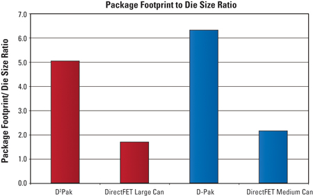
In figure 3, the ideal ratio would tend towards 1, giving the least mm2 of PCB footprint to achieve a given RDS(on). However figure 3 clearly shows the area overhead that the more traditional packages such as the DPak and D2Pak place on the die size area, and ultimately the reduction in current density. The D2Pak has a package footprint to maximum die size area ratio of 5; the package area is five times the size of the largest die size. The Large Can DirectFET however offers a ratio of around 1.7 - so ultimately on the PCB you can achieve a given RDS(on) in a smaller space and therefore at a higher current density as well as saving on PCB and enclosure space. Drawing the factors of space, RDS(on) and RthJA together, table 1 (using equation 4) makes a side by side comparison of a low RDS(on) D2pak product with a counterpart Automotive DirectFET product. The table summarizes the improvement in current density.
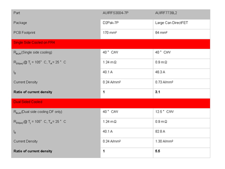
By taking two high performance 40V power MOSFETs which are typically used in automotive applications table 1 shows how current density can be improved by over 3 times due to the low package resistance and small PCB footprint of the DirectFET package. When dual sided cooling is employed the DirectFET can further improve its margin to over 5 times the current density of the D2Pak. The adoption of new fuel efficient vehicles has been kick-started by financial, environmental and political forces of the last few years. But the electrification of the car will only be a long term success if new electrical solutions prove they can overcome the technical and practical dominance of the existing internal combustion engine and its drive train. This has proven to be too greater hurdle over the last 170 years, but today, with highly efficient, cost effective & compact power semiconductors and battery technology the links to the successful electrification of the car are beginning to connect. The humble package which holds the small and delicate semiconductor it important to protect the device from its environment but it also serves an important role as the performance gatekeeper between the die and the PCB. As tougher performance goals are set bringing the packaging technology of power semiconductors up to date will be key to unlock the maximum performance from existing silicon MOSFETs and the next generation compound semiconductors. www.irf.com


