Next-Generation Battery Management System Architectures
New technologies have made significant headway in maximizing electric vehicle range, but charging speed remains a concern
Next-Generation Battery Management System Architectures
DC fast chargers take between 30 to 45 minutes to charge the battery to 80 percent. This fast charging process generates a significant amount of heat, because the internal resistance to the high current generates a temperature rise. For a typical 400 V EV battery, therefore, the charging rate is limited by several factors, like the cross sectional area of the charging cable or the battery cells’ temperature. Some DC fast charger stations liquid-cool the cables to manage their temperature rise caused by I²R power loss. Therefore, increasing the voltage to boost the power delivered rather than the current would seem reasonable.
Porsche’s Taycan EV is the first production vehicle from a major carmaker with a system voltage of 800 V instead of the usual 400 V. A 350 kW Level 3 ultra-fast charging station could potentially allow an 80 percent charge in as little as 15 minutes. However, an 800 V EV design requires new considerations for all electrical systems, explicitly relating to the battery management system.
Consequences of Higher Voltages
More Contactors and Higher Specifications
Main contactors electrically isolate and reconnect the battery and traction inverter when the vehicle is switched off and on. Independent contactors connect and disconnect the battery to and from the DC-Link and charger buses. Additional DC charge contactors are used for DC fast charging to establish the connection between the DC charging station and the battery. There are also auxiliary contactors for the electrical heater for the passenger compartment and the battery heater to optimize efficiency in cold weather conditions.
One of the concerns of moving to higher voltages is the greater potential for damaging electrical arcs. At 800 V architectures, stricter requirements for isolation are required than those traditionally used in 400 V architectures, increasing the solution cost.
Click image to enlarge
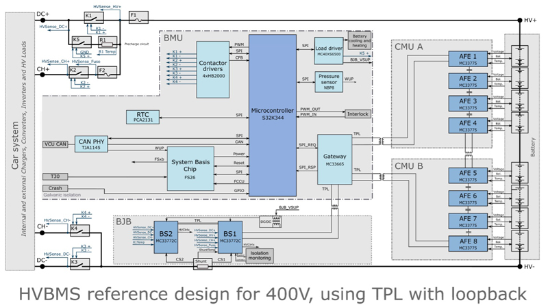
Figure 1: 400 V block diagram
Connector Creepage and Clearance Distances
At higher voltage levels, greater creepage and clearance distances between the connector’s pins are needed to ensure that there is no risk of arcing. Various connector manufacturers have overcome these issues, though they come at a higher price than the 400 V connectors, affecting the total costs.
Drivetrain Components
The ratings of the components in the traction inverter module depend on the maximum battery voltage. If the maximum battery voltage is raised up to 800 V, the availability of suitably rated components diminishes greatly, mostly offered at a premium price. For 400 V batteries, there is a wide selection of these components, keeping the traction inverter module competitively priced.
Different battery architectures come with their inherent advantages and disadvantages. One of the solutions for this challenge is to use two independent 400 V batteries. They can be connected in series when charging (800 V in total), drastically reducing the charging time, and in parallel when driving (400 V). This keeps the cost for the traction inverter module low and allows reusing it in different vehicle models.
Increased Complexity and Functional Safety
Increasing the battery voltage from 400 V to 800 V comes with the unavoidable fact of using more cell sensing devices, or battery cell controllers (BCCs). More devices cause a functional safety challenge since the failure-in-time (FIT) probability is increased. However, the maximum residual FIT for the BMS solution recommended by the ISO 26262:2018 standard does not change.
The BCCs receive only a certain budget of the total allowed system FIT, which cannot be drastically increased. If the FIT budgets were increased, it would affect the budget for the rest of the system, bringing more challenges in other areas by shifting the problem from one place to another.
Switching from 400 V to 800 V for charging
A concept that overcomes most of the challenges mentioned above is a switchable architecture that changes the battery from its native 400 V to 800 V for charging. The battery pack consists of two 400 V batteries; these are connected in parallel during everyday usage to allow the use of standard high-volume 400 V drivetrain components like the inverter and on-board-charger. Capacity and thus range remain unaffected. The BMS switches the two batteries to a series configuration during charging, bumping up the voltage to 800 V, lowering the current, and accelerating charging time. NXP is ready to support OEMs developing these switchable architectures today.
Common hardware and software support scalability
S32K3xx BMS processors
The NXP S32K3xx series of controllers support both 400 V and 800 V architectures and the new switchable architecture. Devices in this series share common peripherals and pin-out, allowing developers to migrate easily within a chip series or among other processors within the S32K portfolio to take advantage of more memory or feature integration, maximizing hardware and software reuse, and reducing time-to-market.
MC33665 BMS gateway
Designers can create more flexible and efficient architectures using the NXP S32K3xx BMS processors in conjunction with the MC33665 BMS transceiver/gateway IC. The device also allows standardization of communication within the battery to CAN-FD compared to the proprietary electrical transport protocol link (ETPL) communication solutions used today.
By standardizing on CAN-FD, OEMs have a single, generic battery management unit (BMU) instead of multiple custom BMUs, reducing costs and time-to-market for new battery models. The MC33665 acts as a transceiver and a gateway. Mounted on the BMU, the device bundles the communication with the battery junction box (BJB) and cell monitoring units (CMUs). Thanks to the four ETPL*lines, the device can establish multiple daisy chains to connect a number of CMU boards and handle all communication and message routing, reducing the computing power load on the MCU. This capability eases the synchronization of the battery pack current and cell voltage measurements performed in their respective functional modules, which then calculates the impedance of the cells and battery pack. In addition, having loopback capability improves the robustness of the communication circuit inside the battery solution.
This software-defined solution disconnects the application layer software from the physical module or cell-to-pack configuration. Different module cell counts are catered for with a scalable battery cell controller (BCC) portfolio from the NXP MC3377X family, ranging from 6 to 18 cells. This flexibility caters to diverse market requirements within the automotive industry.
NXP has developed new devices with a reduced FIT probability to overcome the functional safety challenge. The failure modes’ diagnostic coverage increases by implementing new functional safety concepts, detection methods, and safety architectures, drastically reducing the residual FIT to acceptable levels to support higher voltage solutions.
Best of both worlds
The 2x400 V/800 V switchable battery architecture provides OEMs with the best of both worlds - long-range and ultra-fast charging - without additional drivetrain component costs. It also enables OEMs to add flexibility to their brands by offering models at 400 V or 800 V and benefitting from of economies of scale.
As a full system provider to Tier1 suppliers, NXP offers a scalable and complete chipset solution that supports BMS functions regardless of the chosen architecture. By offering a comprehensive high-voltage BMS (HVBMS) reference design that follows the complete V-Model of the ISO 26262:2018 automotive functional safety standard, NXP helps developers overcome some challenges derived from the new architectural proposals.