Advanced solutions can minimize charging periods & extend runtime
The rapid advances being made in handheld consumer products, such as smartphones, netbooks, and tablet PCs are placing increasingly stringent demands on the Li-ion batteries that act as their power source. Engineering teams need to contend with users’ desires for prolonged run times, as well as the increasing power budget requirements that come with further features and functionality being added to the products they develop.
As a result, far better battery management needs to be implemented. Let’s examine how innovative semiconductor technology now emerging will allow this to be achieved - showing how engineers will thus be able to reduce charging time and also simplify their system designs, while increasing the lifespan of the battery and lengthening discharge times.
Across the globe OEM power system design engineers are striving to extract more performance from a single cell Li-ion battery over a very wide range of temperatures and load values. In order to achieve this goal, critical system parameters must be tightly controlled under all conditions - including conduction losses which must be aggressively reduced. The greater precision with which these system parameters are controlled the higher the performance level obtained from the battery.
Demands are increasing
The public demand for more sophisticated portable electronics devices is not being abated. New products are being introduced all the time with:
1. Greater feature sets, so that OEMs can differentiate themselves from their rivals in what are extremely competitive markets. This of course effects the overall power budget - for example inclusion of GPS and Bluetooth will both present significant drains to the battery.
2. Displays with ever-larger dimensions being incorporated. Early cell phone models only required rudimentary displays. With the advent of smartphones however this all changed, as sizeable touch-enabled thin-film transistors (TFTs) became the basis of these products’ user interfaces. Subsequent generations of smartphone have employed bigger and bigger display formats, with certain models now looking to fill the gap that lies between them and tablet PCs. In some cases they are using up to 6.3-inch diagonals.
Though users want the benefits of all this extra functionality and larger screens they are not willing to compromise in any way on either the length of time between recharges or how quickly these recharges take to complete. Given that the battery technology has not really improved too greatly over the last decade, the quantity of charge that batteries of a given format can store has stayed relatively constant. Engineers, as a result, must concentrate their efforts on increasing the charge rate that can be supported.
The charge rate of a battery - which is denoted by C - quantifies the capacity that the battery has to store electrical charge over the course of an hour of charging. It is now increasingly common for portable products to have a full charge rate of 1C (i.e. charging of the battery is completed within an hour) or even 2C (i.e. it is completely charged in just 30 minutes).
With the charge rate of portable products being introduced onto the market seeing a widespread increase, the stress that the constituent electronics will be under is becoming exacerbated. The temperature dependence of the on-state resistance of the components in the power system is critical. The on-state resistance of components - which is symbolized by RDS(on) - will increase a lot if the value of C is raised, leading to the adapter becoming hotter.
In order to combat this, more comprehensive thermal management will be needed to ensure that operational reliability is maintained. This is something that OEMs want to avoid. Firstly because it increases the adapter size, which goes against the sleek low-profile designs that OEMs want to utilize as they will be more attractive to consumers. Secondly it increases the overall cost, which is equally problematic in the price-sensitive markets that these OEMs are situated.
The challenge is to be able to raise C while still having acceptably low values of RDS(on) for key components within the system. An additional issue is that most of these devices are manufactured in extremely high volumes. Each portable product needs to have the same performance, so component sorting is needed. Sorting is based on average operational conditions and does not take into account extremes of temperature. This further constricts the available window of operation for the Li-ion battery.
A novel approach to charging system circuit protection
Engineers need to efficiently manage both the charge and discharge current within charging systems whilst at the same time protecting their Li-ion batteries from the potential harm that is posed by over-voltage, over-current and over-temperature phenomena. The protection circuitry between the Li-ion battery and the rest of the portable product will traditionally include a power MOSFET and some basic control circuitry.
One of the most significant dynamics the charging system hinges on is the way that temperature effects the power MOSFET’s RDS(on). As already mentioned there is a need to lower RDS(on) so that heightened battery charging rates can be realized without increasing the heat levels present.
The key to solving the problem is the specification of more highly integrated semiconductor devices. Co-packaged solutions are now emerging, with both the circuit protection and power MOSFET elements included. In principal these can resolve many of the issues discussed and save space too. Chip scale package (CSP) format devices provide the lower RDS(on) values that are needed to enhance system designs. Furthermore better bonding technologies are also proving beneficial, with clip bonding rather than conventional wire bonding being considerably more effective.
Though several co-packaged solutions are already available, generally they lack certain attributes, which are going to be of major importance in next generation charging system designs. This is because they don’t have access to a built-in temperature sensor, so they aren’t able to offer the current monitoring functionality that will be essential if system reliability is to be fully maintained.
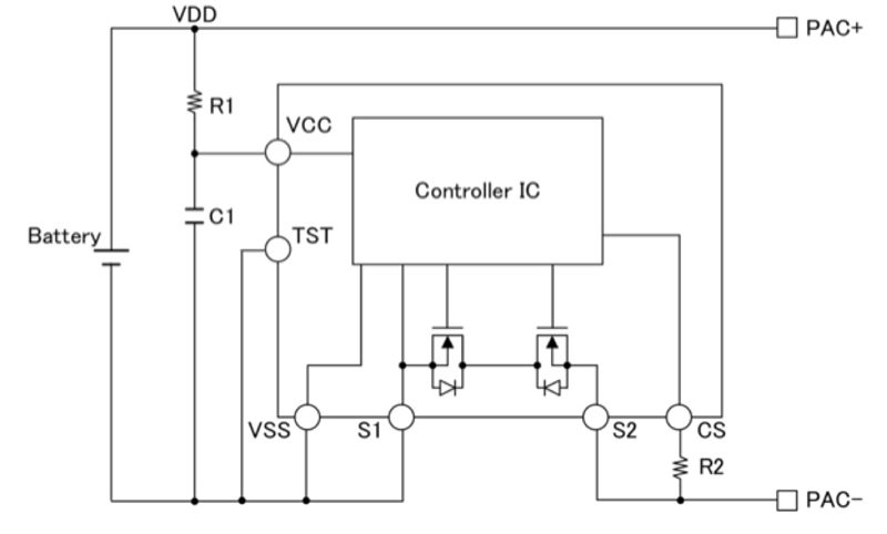
For example, the LC05111CMT from ON Semiconductor, is a highly advanced protection IC targeted especially at single cell Li-ion battery charging applications. Thanks to its high degree of functionality, it can be used to construct circuit protection systems with only a few additional external components. It has two integrated power MOSFET elements, as well as highly accurate detection/detection delay circuitry, which prevents batteries from over-charging, over-discharging, over-current discharging and over-current charging. Figure 1 shows this device in-situ.
Click image to enlarge
Figure 1: Application Circuit using ON Semiconductor’s LC05111CMT
While in normal mode it controls charging/discharging by detecting cell voltage (VCC) and CS pin voltage. If the cell voltage is between the over-discharge detection voltage (Vuv) and over-charge detection voltage (Vov), and the CS pin voltage is between charging over-current detection voltage (Voc1) and over-discharge detection voltage, then the power MOSFET elements are turned on. By decreasing the Li-ion battery temperature, more accurate over-current protection and a lowering of the Rss(on), which is the combined RDS(on) of the two power MOSFET elements, can be attained.
Expedient, rapid charging will be fundamental in the consumer electronics products of the future, but it comes with increased risk of overheating. This means that more advanced protection mechanisms are going to be required. Through the integration of the power MOSFET and the control circuit, as described here, along with advanced thermal management and precision sensing, it will be possible to significantly reduce the total tolerance in the interface circuit while lowering the RDS(on) of the power MOSFET aspect too. This substantially increases the total usable range of load voltage and current while also improving manufacturing yields (and thereby reducing unit costs).