Author:
Tony Armstrong, Director of Product Marketing, Power Products, Linear Technology Corporation, tarmstrong@linear.com
Date
01/09/2018
 PDF
PDF
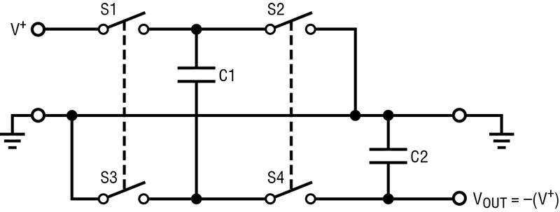
Figure 1. Simplified Charge Pump Block Diagram of a Voltage Inverter
A fundamental axiom for switching power supplies is that they must not generate a lot of noise. Accordingly, quiet, well-regulated power supplies are important for optimum performance in many circuit applications. In order to attain this level of performance it is critical to be able to mitigate any noise generated as part of this conversion process. An obvious way to attain this is to simply use a linear regulator. However, although they supply quiet power supply rails, their conversion efficiencies are poor at high step-down ratios and this can lead to thermal issues with the design in high output current applications.
Of course, magnetic-based switching regulators can alleviate the usual thermal issues since they generally have high efficiency of conversion, leading to simpler thermal design when high output currents are required by the end application. It is well understood that component selection and circuit board layout can play a significant role in determining the success or failure of virtually all power supplies. These aspects set their functional EMI and thermal behavior. For the un-initiated, switching power supply layout may seem like a “black” art, but it is in fact a basic aspect of a design often overlooked in the early stages of the process. Since functional EMI requirements always have to be met, what is good for functional stability of the power supply is also usually good for its EMI emissions, too. Furthermore, good layout from the beginning does not add any cost to the design and can actually provide cost savings by eliminating the need for EMI filters, mechanical shielding, EMI test time and numerous board revisions.
Moreover, the potential problems of interference due to noise can be exacerbated when multiple DC/DC switchmode regulators are used in a design to generate multiple rails or if they are paralleled for current sharing and higher output power. If all are operating (switching) at a similar frequency, the combined energy generated by multiple regulators in a circuit is then concentrated at one frequency. Presence of this energy can become a concern, especially if the rest of the ICs on the printed circuit boards (PCBs), as well as other system boards are close to each other and susceptible to this radiated energy. This can be particularly troubling in industrial and automotive systems that are densely populated and are often in close proximity to electric noise generating sources, such as mechanically switched inductive loads, PWM drive power outputs, microprocessor clocks and contact switching. Furthermore, if switching at different frequencies, intermodulation products can alias into sensitive frequency bands.
Switching Regulator Emissions
Switching regulators usually replace linear regulators in areas where low heat dissipation and efficiency are valued. Moreover, the switching regulator is typically the first active component on the input power bus line, and therefore has a significant impact on the EMI performance of the entire product design.
Conducted emissions ride on the wires and traces that connect up to a product. Since the noise is localized to a specific terminal or connector in the design, compliance with conducted emission requirements can often be assured early in the development process with a good layout or filter design. Radiated emissions are a different matter altogether. Everything on the board that carries current radiates an electromagnetic field. Every trace on the board is an antenna and every copper plane is a resonator. Anything, other than a pure sine wave or DC voltage, generates noise all over the signal spectrum. Even with careful design, a power supply designer never really knows how bad the radiated emissions are going to be until the system is tested. And radiated emissions testing cannot be formally performed until the design is essentially complete.
Filters are often used to reduce EMI by attenuating the strength at a certain frequency or over a range of frequencies. A portion of this energy that travels through space (radiated) is attenuated by adding metallic and magnetic shields. The part that rides on PCB traces (conducted) is tamed by adding ferrite beads and other filters. EMI cannot be eliminated but can be attenuated to a level that is acceptable by other communication, signal processing and digital components. Moreover, several regulatory bodies enforce standards to ensure compliance in both industrial and automotive systems.
Modern input filter components in surface mount technology have better performance than through-hole parts. However, this improvement is outpaced by the increased demands created by today's high frequency switching regulators. The low minimum on and off times required at higher operating frequencies result in higher harmonic content due to the faster switch transitions, thereby increasing radiated noise. However, these high switch edge rates are needed to get higher conversion efficiencies. A switched capacitor charge pump does not exhibit this behavior since it operates at much lower switching frequencies and most importantly can tolerate slower switching transitions without degradation in efficiency.
Savvy PCB designers will make the hot loops small and use shielding ground layers as close to the active layer as possible. Nevertheless, device pin-outs, package construction, thermal design requirements and package sizes needed for adequate energy storage in decoupling components dictate a minimum hot loop size. To further complicate matters, in typical planar printed circuit boards, the magnetic or transformer style coupling between traces above 30MHz will diminish all filter efforts since the higher the harmonic frequencies are, the more effective unwanted magnetic coupling becomes.
Switched Capacitor Charge Pumps
Charge pumps have been around for decades, and they provide DC/DC voltage conversion, using a switch network to charge and discharge two or more capacitors. The basic charge pump switch network toggles between charge and discharge states of the capacitors. As shown in Figure 1, C1 the “flying capacitor” shuttles charge, and C2 the “reservoir capacitor” holds charge and filters the output voltage. Additional “flying capacitors” and switch arrays enable multiple gains.
When switches S1 and S3 are on, or closed, and switches S2 and S4 are off, or open, the input power supply charges C1. During the next cycle, S1 and S3 are off, S2 and S4 are on, and charge transfers to C2, generating VOUT = - (V+).
However, until recently, charge pumps have had limited input and output voltage ranges, which has limited their use in industrial and automotive applications where inputs up to 40V or greater are commonplace.
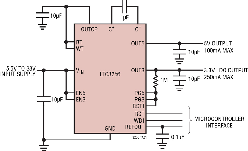
A recent introduction in this area is Linear Technology’s LTC3256. It is a highly integrated, high voltage low noise dual output power supply, which takes a single positive input and generates 5V and 3.3V step-down supplies with high efficiency and no inductors. The device features a wide 5.5V to 38V input voltage range and includes independently enabled dual outputs: a 5V 100mA supply, and a 250mA 3.3V low-dropout (LDO) regulator, for a total of 350mA output current. This combination of regulators offers much lower power dissipation than a dual-LDO solution. For example, with a 12V input and a maximum load on both outputs, power dissipation is decreased by over 2W with the LTC3256 vs. a dual LDO, thus reducing the heat loss and input current. See Figure 2 for its complete schematic.
Click image to enlarge
Figure 2. LTC3256 Schematic Has a 5V/100mA Output & a 3.3V/250mA Output
The LTC3256 has been engineered for diagnostic coverage in ISO26262 systems and incorporates numerous safety and system monitoring features. The device is well-suited for a variety of applications requiring low noise, low power rails from high voltage inputs such as automotive ECU/CAN transceiver supplies, industrial/telecom housekeeping supplies, and general-purpose low-power conversion.
The LTC3256 maximizes efficiency by running the charge pump in 2:1 mode, over as wide an operating range as possible, and automatically switches to 1:1 mode as needed, consistent with VINand load conditions. Controlled input current and soft switching minimize conducted and radiated EMI. The device offers low quiescent current of only 20μA with both outputs in regulation (no load) and 1μA in shutdown. The integrated watchdog timer, independent power good outputs and reset input ensure reliable system operation and enable fault monitoring. A buffered 1.1V reference output enables system self-testing diagnostics for safety critical applications. The LTC3256 also has additional safety features including overcurrent fault protection, over temperature protection and tolerance of 38V input transients.
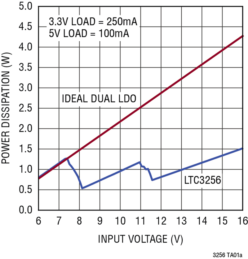
The graph of Figure 3 below highlights the LTC3256’s good power dissipation characteristics. At 12VIN, the LTC3256 with 3.3V @250mA and 5V @100mA outputs dissipates about 750mW, while under these same conditions, a dual LDO would dissipates almost 3W. That’s 2.25W less for LTC3256, which is a huge benefit for the thermal aspect of the design.
Click image to enlarge
Figure 3. Power Dissipation Characteristics of the LTC3256 vs. a Dual LDO
Conclusion
It is well known that EMI considerations require careful attention during the initial design process in order to ensure that they will pass EMI testing once the system is completed. Until now, there has been no sure fire way to guarantee that this could easily be attained with the right power IC selection for all but very low power systems. However, with the recent introductions of low EMI regulators, such as the LTC3256 high voltage charge pump, an alternative choice is now available. It provides much higher efficiency and lower power loss when compared to linear regulators and do not require the compensation, layout, magnetics and EMI issues associated with a switching regulator.