Enabling the real performance of GaN by using dedicated gate driver technology
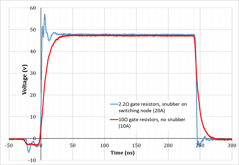
Figure 1: Switching waveforms using a moderate switching speed of ca. 5-10ns and a fast switching speed of ca. 1-2ns for 48V to 3.3V conversion at 300kHz
Since the introduction of the first gallium nitride (GaN) transistors over ten years ago, their advantages in power electronics over silicon MOSFETs have become well-known. Indeed, the material properties of GaN offer lower parasitic capacitances for a given on-resistance, inherent fast switching transients, lack of reverse recovery and high temperature operation capability. These excellent properties are seemingly the perfect combination for high performing power converters.
However, for optimal performance of the GaN technology, the gate-drive needs to be optimized. The gate-source voltage is to be controlled in tight windows of both voltage and time. Considering a typical half-bridge, this implies high-side gate-source voltages floating up and down at high voltage (e.g. 200V) and at high dV/dt (e.g. 100V/ns). Such stringent operating conditions require optimized and dedicated gate driver technology.
Solving GaN gate-driving pitfalls with the MDC901
GaN transistors in power applications have a lot of potential, including higher power efficiency, higher power density, potential heatsink/fan-less designs, and more. However, getting the maximal benefit from a GaN stage requires careful driving, avoiding the pitfalls along the road.
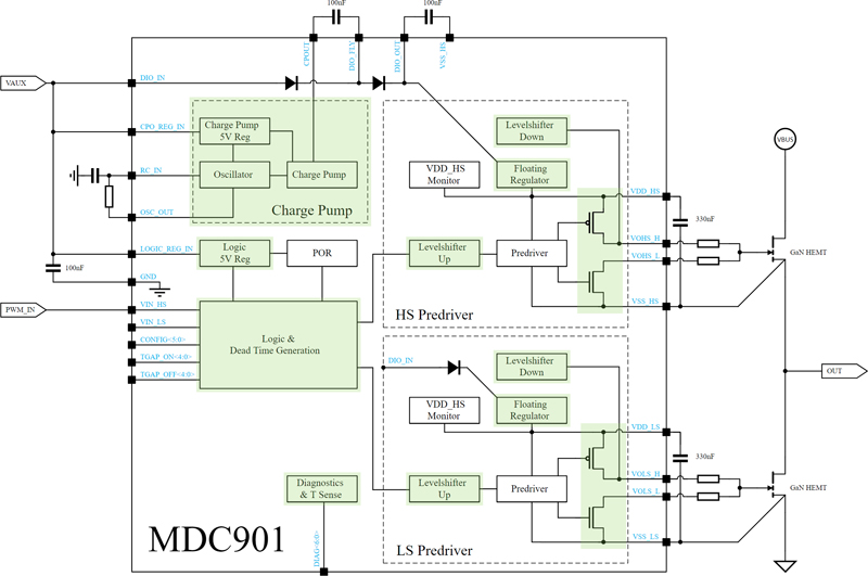
For this reason MinDCet introduced the MDC901 GaN gate driver. The depicted block diagram in Figure 2 provides an overview of the key functionality, solving the major pitfalls when driving GaN devices.
Click image to enlarge
Figure 2: The block diagram of the MDC901 GaN gate driver
High Slew Rates
One of the big benefits of GaN power stages is their fast switching ability to switch, potentially leading to very low switching losses. The quick switchover between low and high-side transistors causes the load current to alternate very quickly, putting constraints on the bus voltage decoupling and its parasitic bus loop inductance.
The MDC901 has separate pull-up and pull-down paths, to allow for tuning of the slew-rate of the output stage, while maintaining a low impedance pulldown path for the GaN transistor to avoid parasitic turn-on.
Deadtime
Deadtime in a half-bridge is the time between the turn-off event of one transistor and the turn-on event of the complementary bridge transistor. For optimal efficiency, the deadtime needs to be tuned for a given application.
The MDC901 has separate deadtime control for turn-on and turn-off can through a series of digital inputs. This allows tuning of the deadtime for a given application, either static or dynamically. Additionally, a fail-safe operation mode is present, which sets the deadtime based on sensing the GaN gate voltage.
Gate Overcharging
In non-isolated gate-drive applications, the gate driver is supplied through bootstrapping of the low voltage supply. This technique will charge the high-side gate driver supply decoupling capacitor through a fast high-voltage diode. Inductive voltage spikes or non-zero deadtime will cause negative half bridge output voltages, which could lead to detrimental overcharging for the GaN gate.
The MDC901 avoids the risk of gate-overcharging during negative voltage operation by placing fully floating regulators both in the high-side and low-side domain after the bootstrap diode. This results in a well defined and robustly protected gate driver voltage.
Negative Output Voltage Operation
The negative swing of the output driver voltage depends on the parasitic source inductance and the load conditions of the power converter, which can be poorly predicted. For predictable operation, a guarantee that the converter bridge can always be controlled is required, even when entering negative voltage relative to the supply grounds.
The MDC901 allows for guaranteed negative output voltage operation down to -4V, allowing accurate gate control even under high inductive currents. This has been accommodated by a specifically designed level shifter and floating supply generation.
High duty cycle operation
Bootstrapped operation of a gate driver is a simple and effective means to provide charge to control the high-side transistor, for example, in a half-bridge. Unavoidably, the bias for supporting circuitry needed in the predriver system - which causes the bootstrap voltage to leak away, sets a maximum on the duty cycle that can be maintained or limits the modulation depth that can be used.
For high duty cycle applications (e.g. motor drivers and class-D amplifiers), it is mandatory to maintain a high-side on-state for longer periods of time. This functionality was implemented in the MDC901 by an integrated charge pump, compensating for DC bias under 100% duty cycle conditions.
The MDC901 provides a high-end and feature-rich solution to driving GaN transistors in a reliable way for maximizing performance in the given application with a clean and fast switching node voltage. The driver was developed for DC-DC solutions, but can be used for all other GaN driving applications like LIDAR, motor drivers, and electronic fuse applications requiring true 200V capability.
User Experience of the MDC901 Evaluation Board (EVB)
The dedicated evaluation board (MDC901-EVBHB) allows the user to experience the capabilities of the gate driver in real life. The MDC901-EVBHB, hereby referred to as EVB, consists of a buck converter built around the MinDCet MDC901 gate driver, a GaN Systems GS61008P half-bridge and a WE-HCF 1.4uH/31.5A power inductor, as depicted in Figure 3. Implementations using different GaN technology flavours and topologies are under development and available upon request.

Click image to enlarge
Figure 3: The MDC901 100V half-bridge evaluation board (MDC901-EVBHB)
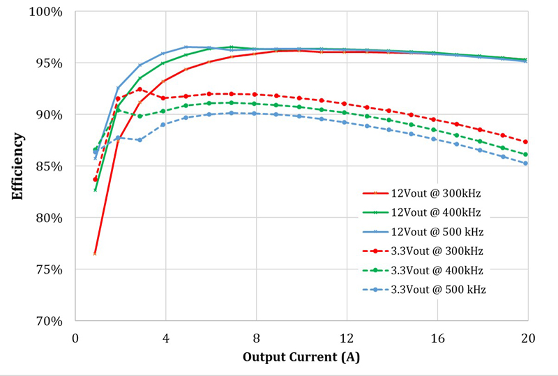
The power of GaN can be demonstrated with a high input/output ratio buck converter. As an example, we have measured a 48V to 3.3V use-case, using the EVB. The low duty cycle (ca. 6.9%) benefits from the fast switching transient speeds, resulting in a 10 to 15 percent efficiency increase over an equivalent MOSFET-based converter at the same switching frequency. The efficiency measurement in Figure 4 exemplifies that despite GaN’s capabilities, the conversion efficiency decreases as switching frequency increases. Already at moderate switching frequencies of 300 kHz, a clear decrease of nearly 1 percent efficiency per additional 100 kHz in switching frequency can be observed over the measured frequencies from 300 to 500 kHz. This contradicts the high-frequency GaN paradigm and indicates that the higher efficiencies possible with GaN is not necessarily achieved at higher frequencies. Although, this may depend on the actual voltages and their ratio. Looking at the 12V output case, the efficiency is not notably affected in this frequency range at moderate to high output loads. In fact, the efficiency benefits from the higher switching frequency at low loads due to the reduced ripple current in the inductor, which in-turn yields lower AC-losses in the inductor and lower Rdson losses in the GaN switches.
Click image to enlarge
Figure 4: The measured efficiency as a function of the output current for a 48V to 3.3V and 48V to 12V GaN-based buck converter, at different switching frequencies
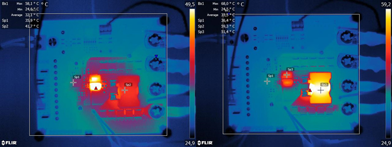
Even the best DC-DC converter experiences losses which must be dissipated in an efficient manner. Our EVB comes with a pushpin, forced-air heat sink that installs on the EVB backside. The fan can be chosen to be powered or not depending on the actual ambient temperature and power level. Thermal images are shown in Figure 5, with respective setpoints of 48V in, 3.3V and 12V out, both at 20A load current and a switching frequency of 300kHz. The resulting in an efficiency of 88.6% and power dissipation of 8.5W for the 3.3V case and an efficiency of 95.3% and power dissipation of 11.8W for the 12V case. In this situation, it can be observed that the main power is being dissipated in the actual GaN power stage for the 3.3V case and mainly by the inductor in the 12V case. The MDC901 is mainly heated by conduction from the GaN HEMTs in the 3.3V case. This clearly demonstrates that depending on the use case the power dissipation distribution may shift between inductor and GaN switches. Moreover, it shows for the 3.3V case that the driver needs to be able to cope with increased operating temperatures since it is in close proximity of the GaN.
Click image to enlarge
Figure 5: The thermal images of the MDC901-EVBHB for 48 V to 3.3V (left) and 12V (right) GaN-based buck converter use cases with an output current of 20A
Conclusion
Enabling the true benefits of GaN power stages requires implementing an optimized gate driver that is designed specifically to work with GaN transistors. Resultantly, the GaN can be pushed to the limits, yielding the highest possible performance, which provides for a maximum return on the technological and monetary investment. A discrete gate driver such as the MDC901 provides the user with the flexibility, diagnostics and an expanded feature set for choosing the best-suited GaN transistors for the given application.


.jpeg)
 Single.jpeg)
