Noise Sensitive Applications Want Ultralow Noise LDO Regulators
Low dropout linear regulator (LDO) is a special type of linear regulator
Linear Regulators are integrated circuits that step a voltage down from a higher voltage to a lower voltage without the need of an inductor. The low dropout linear regulator (LDO) is a special type of linear regulator in which the dropout voltage – the differential between the input-to-output voltages needed to maintain regulation – is typically below 400mV. Early linear regulator designs offered dropouts on the order of ~1.3V, meaning for a 5V input, the maximum achievable output was only ~3.7V for the device to stay in regulation. More recently, “low” dropout is considered to be 500mV or less. Nevertheless, in these days of more sophisticated design techniques and wafer fabrication processes, “low” dropout is typically <100-300mV or so.
Furthermore, although the LDO is rarely the most expensive system component in any given system, it is often one of the most valuable components from a cost/benefit basis. One of the LDO’s tasks is to protect expensivedownstream loads from harsh environmental conditions such as voltage transients, power supply noise, reverse voltage, current surges, etc. In short, its design must be robust and also contain all of the protection features needed to “absorb the punishment” from its environment while protecting the load. Many low-cost LDO linear regulators do not have the necessary protection features and thus fail, often causing damage not only to the regulator itself, but also the downstream load.
LDOs vs Other Regulators
Low voltage step-down conversion and regulation can be achieved via a variety of methods.
Switching regulators operate with high efficiency over a wide range of voltages but require external components such as inductors and capacitors for operation, thus taking up a relatively larger board space. Inductorless charge pumps (or switched capacitor voltage converters) can also be used to achieve lower voltage conversion but are limited in output current capability, suffer from poor transient performance, and require more external components versus a linear regulator.
Today’s generation of fast, higher current, low voltage digital ICs such as FPGAs, DSPs, CPUs, GPUs and ASICs, have placed stringent demands on supplies that power the core and I/O channels. Traditionally, efficient switching regulators have been used to power these devices but they can have potential noise interference issues, transient response and layout limitations. As a result, LDOs are becoming an alternative in these applications, as well as other low voltage systems. Thanks to recent product innovations and feature enhancements, LDOs offer some performance benefits that make them more desirable.
Furthermore, when it comes to powering noise-sensitive analog/RF applications (such as commonly found in test and measurement systems, where the measurement accuracy of the machine or equipment needs to be orders of magnitude better than the entity being measured), LDOs are generally preferred over their switching counterparts. Low noise LDO regulators power a wide range of analog/RF designs, including frequency synthesizers (PLLs/VCOs), RF mixers and modulators, high speed and high resolution data converters (ADCs and DACs) and precision sensors. Nevertheless, these applications have reached sensitivities that are testing the limits of conventional low noise LDOs. For instance, in many high-end VCOs, power supply noise directly affects the VCO output phase noise (jitter). Moreover, to meet overall system efficiency requirements, the LDO usually post-regulates the output of a relatively noisy switching converter, so the high frequency power supply ripple rejection (PSRR) performance of the LDO becomes paramount.
LDO Design Challenges
Plenty of industry standard linear regulators perform the low dropout operation with a single voltage supply, yet most cannot achieve the combination of very low voltage conversion with low output noise, wide ranging input/output voltages and extensive protection features. PMOS LDOs achieve the dropout and run on a single supply but are limited at low input voltages by the pass transistor’s Vgs characteristics as well as lack the many protection features from high performance regulators. NMOS-based devices offer fast transient response but require two supplies to bias the device. NPN regulators offer wide input and output voltage range but either require two supply voltages or have higher dropout. By contrast, with the proper design architecture, a PNP regulator can achieve low dropout, high input voltage, low noise, high PSRR and very low voltage conversion with bulletproof protection and all from a single supply rail.
For best overall efficiency, many high performance analog and RF circuits are powered from LDOs post-regulating the output of a switching converter. This requires high power supply ripple rejection (PSRR) and low output voltage noise at low input-to-output differentials across the LDO. An LDO with high PSRR easily filters and rejects noise from the switcher’s output without requiring bulky filtering components. Further, a device with low output voltage noise across a wide bandwidth is beneficial for today’s modern rails where noise-sensitivity is a key consideration. Low output voltage noise at high currents is clearly a necessary specification.
New Ultralow Noise, Ultrahigh PSRR LDO Family
It is clear that a LDO solution that solves the issues outlined herein should have the following attributes:
- Very low output noise
- Low dropout operation
- High PSRR across a broad range of frequencies
- Single supply operation (for ease of use and relaxed supply sequencing challenges)
- Fast transient response time
- Operation over a wide input/output voltage range
- Moderate output current capability
- Excellent thermal performance
- Compact footprint
To address these specific needs, Linear Technology introduced its LT304x family of ultrahigh PSRR, ultralow noise LDO regulators. The newest member is the LT3045, an ultralow noise, ultrahigh PSRR low dropout voltage linear regulator. It is a higher-output current version of the previously released 200mA LT3042 ultralow noise LDO. The LT3045’s unique design features ultralow spot noise of only 2nV/√Hz at 10kHz and 0.8µVRMS integrated output noise across a wide 10Hz to 100kHz bandwidth. Low frequency PSRR exceeds 90dB out to 10kHz and high frequency PSRR exceeds 70dB out to 2.5MHz, thereby quieting noisy or high ripple input supplies. The LT3045 utilizes Linear’s proprietary LDO architecture – a precision current source reference followed by a high performance unity gain buffer, resulting in virtually constant bandwidth, noise, PSRR and load regulation performance, independent of output voltage. In addition, this architecture permits paralleling of multiple LT3045s to further decrease noise, increase output current and spread heat across the circuit board for improved thermal performance.
The LT3045 delivers up to 500mA output current with a 260mV dropout voltage at full load, across a wide 1.8V to 20V input voltage range. Output voltage range is 0V to 15V and output voltage tolerance is highly accurate at ±2% over line, load and temperature. The device’s wide input and output voltage ranges, high bandwidth, high PSRR and ultralow noise performance are ideal for powering noise-sensitive applications such as PLLs / VCOs / mixers / LNAs, very low noise instrumentation, high speed/high precision data converters, medical applications such as imaging and diagnostics, precision power supplies and as a post regulator for switching supplies.
The LT3045 operates with a small, low cost, 10µF ceramic output capacitor, optimizing stability and transient response. A single resistor programs the external precision current limit (±10% over temperature). A single SET pin capacitor lowers output noise and provides reference soft-start functionality, preventing output voltage overshoot at turn-on. Moreover, the device’s internal protection circuitry includes reverse battery protection, reverse current protection, internal current limit with foldback and thermal limit with hysteresis. Other features include fast start-up capability (useful if a large value SET pin capacitor is used) and a power good flag with programmable threshold to indicate output voltage regulation. Figure 1 shows a typical application schematic.
The LT3045 is available in thermally enhanced 10-lead 3mm x 3mm DFN (pin-compatible with the LT3042) and 12-lead MSOP packages, both with a compact footprint. The E- and I-grade versions are available from stock with an operating junction temperature of –40°C to 125°C.
A future high temperature H-grade version will be rated from –40°C to 150°C.
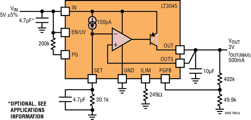
Click image to enlarge
Figure 1. LT3045 Typical Application Schematic & Features
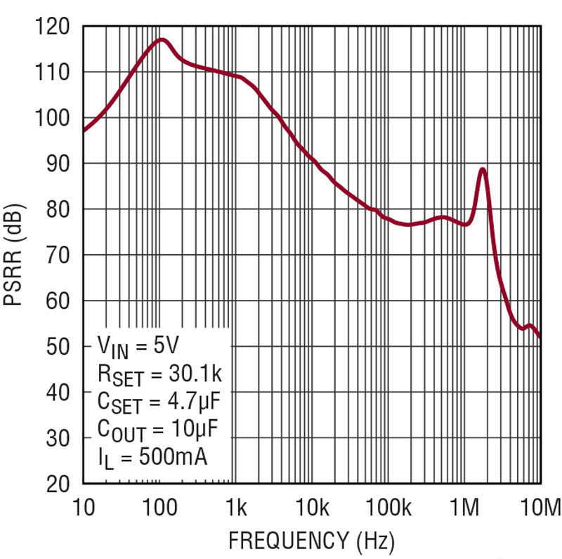
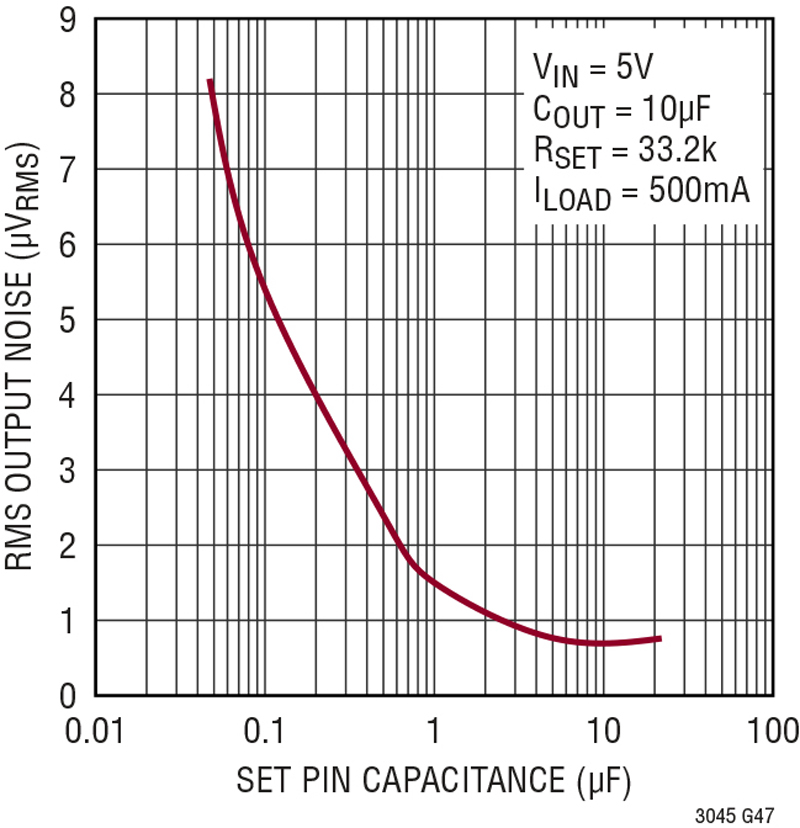
The LT3045 requires an output capacitor for stability. Given its high bandwidth, the device requires low ESR and ESL ceramic capacitors. A minimum 10µF output capacitance with an ESR below 20mΩ and an ESL below 2nH is required for stability. Given the high PSRR and low noise performance (see Figures 2 and 3) attained using a single 10µF ceramic output capacitor, larger values of output capacitor only marginally improve the performance because the regulator bandwidth decreases with increasing output capacitance — hence, there is little to be gained by using larger than the minimum 10µF output capacitor.
Power Supply Ripple Rejection
Click image to enlarge
Figure 2. LT3045 PSRR Performance
Click image to enlarge
Figure 3. LT3045 Output Noise Performance
Benefits of Parallel Devices
Higher output current is obtained by paralleling multiple LT3045 ICs, by simply tying all the SET pins together and all the IN pins together. Connect the OUT pins together using small pieces of PCB trace (used as a ballast resistor) to equalize currents from the LT3045s. More than two LT3045s can also be paralleled for even higher output current and lower output noise. Paralleling multiple LT3045s is also useful for distributing heat on the PCB. For applications with high input-to-output voltage differential, an input series resistor or resistor in parallel with the LT3045 can also be used to spread heat. See Figure 4 for a parallel circuit implementation.
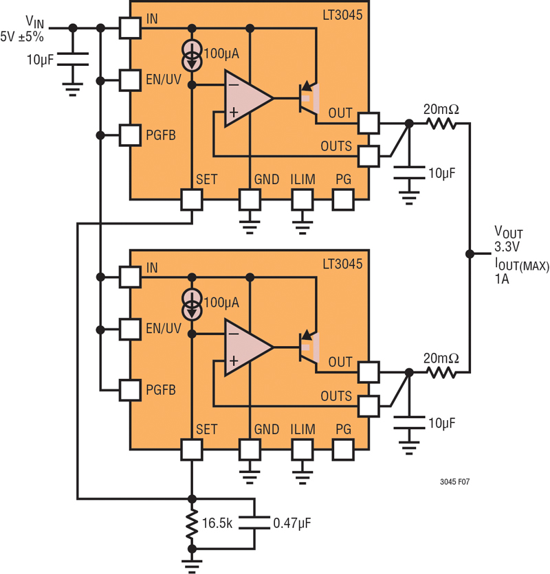
Click image to enlarge
Figure 4. LT3045 Parallel Operation
Table 1 below shows the members of Linear’s ultrahigh PSRR, ultralow noise family of LDOs.
|
Part # |
VIN Range |
VOUT Range |
IOUT |
Dropout Voltage |
PSRR @1MHz |
Output Noise |
Spot Noise |
Packages |
|
LT3042 |
1.8V - 20V |
0V - 15V |
200mA |
350mV |
79dB |
0.8µVrms |
2nV/rtHz |
MSOP-10, 3x3 DFN * |
|
LT3045 |
1.8V - 20V |
0V - 15V |
500mA |
260mV |
76dB |
08µVrms |
2nV/rtHz |
MSOP-12, 3x3 DFN * |
* DFN packages are pin compatible
Table 1. Ultrahigh PSRR, Ultralow Noise LDOs
Conclusion
The LT3042 and LT3045’s breakthrough noise and PSRR performance, coupled with their wide voltage range, low dropout voltage, robustness and ease-of-use, make them ideal for powering noise-sensitive applications such as in test and measurement systems. With their current-reference based architecture, noise and PSRR performance remain independent of the output voltage. Additionally, multiple devices can be directly paralleled to further reduce output noise, increase output current and spread heat on the PCB.