Author:
Kanazawa University
Date
05/22/2018
 PDF
PDF
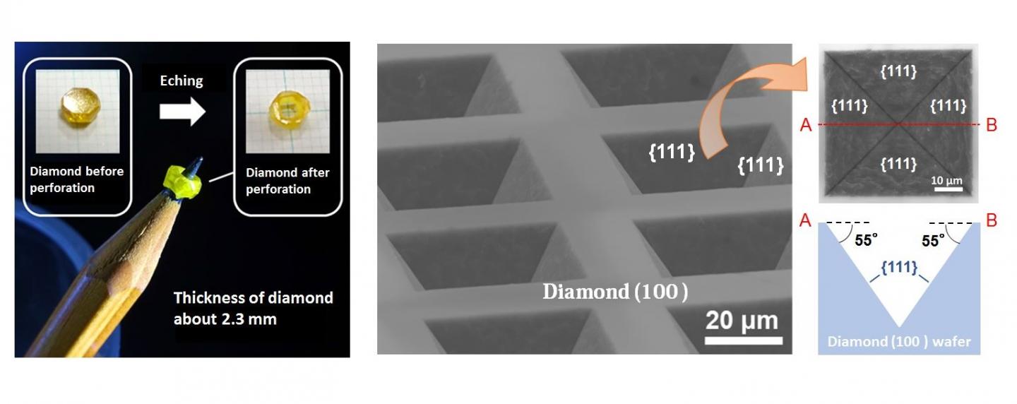
Left: A single crystal diamond with a hole that is perforated by the high-rate etching technique. Center: Single crystal diamond wafer with regular trench structures produced by the anisotropic etching technique. Right: Top view of such a trench structure and a schematic image of its cross-section.
World energy consumption has been increasing year by year, and a global-scale energy shortage is of great concern. Because of this reason, it is important to use the energy (electricity) produced by power generation even more efficiently, the key to which is the development of power devices*1) that control the electric power. The present mainstream Si power devices have been highly developed but their performance is thought to be close to maximum, which means that further development becomes very difficult. Thus, much attention has recently been paid to other materials possessing better physical properties than Si, such as SiC, GaN, Ga2O3 (gallium oxide) and diamond, i.e. wide-bandgap semiconductors*2). Among these, diamond shows not only the highest insulation breakdown voltage*3) and carrier mobility*4) but also larger thermal conductivity than any other material. These are big advantages in realizing power devices with properties of high-voltage endurance, reduced transmission loss, high-speed and miniaturization. Diamond is, therefore, regarded as an ultimate material for power devices with great promise. On the other hand, since diamond possesses extreme hardness and chemical stability, it is not an easy task to fabricate device structures by etching. Although current fabrication technology of diamond power devices uses plasma process*5), not only is the etching rate low but diamond proximal to the etching site is damaged due to the plasma, which deteriorates device performances. Thus, it was desired to develop a non-plasma process that enables diamond etching at a high-rate. In this study, by focusing on the solid-solution reaction*6) of carbon into nickel, we have aimed to develop new diamond etching process.
[Results]
The present study was conducted as a collaborative effort of researchers from the National Institute of Advanced Industrial Science and Technology and researchers from Kanazawa University including doctor-course graduate student Masatsugu NAGAI and Associate Professor Norio TOKUDA. By employing continuous solid-solution reaction of diamond carbon with nickel in high-temperature (1000 °C) water vapor, an anisotropic diamond etching process*7) has been realized at the highest rate (approximately 8.7 μm/min) reported so far (Figure 1). The high-temperature water vapor oxidizes the nickel surface and the solid-solute carbon atoms are converted into carbon dioxide or carbon monoxide by an oxidation-reduction reaction with nickel oxide. Carbon dioxide and carbon monoxide are released from the reaction system, which prevents saturation of carbon atoms in nickel and enables continuous diamond etching at a high rate (Figure 2). In addition, high-temperature water vapor, unlike oxygen, does not react with diamond directly, so that selective etching of diamond in direct contact with nickel is now possible. Moreover, since plasma is not used, this technology does not bring about the plasma damage that deteriorates device performance.
[Future prospects] It is expected that by using the technology developed in this study, diamond power devices with vertical trench*8) gate structures can be fabricated, which should show characteristics of highly reduced transmission loss and high-voltage endurance. In addition, this technology is expected to be applicable not only to fabrication of device structures but also to manufacturing processes like diamond flattering and cutting.
EurekAlert!, the online, global news service operated by AAAS, the science society: https://www.eurekalert.org/pub_releases/2018-05/ku-nha052118.php