Normally-Off and Current Collapse Free by Unique GIT Technology Realize Commercialization of GaN Transistor
Creating MOS alternative devices to address the needs of advanced power systems
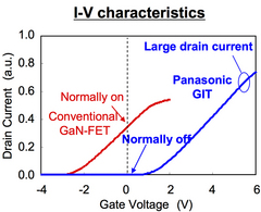
Figure 1: I-V Characteristics of Normally Off GIT GaN and Conventional Normally On GaN
For more than thirty-five years, the power MOSFET dominated the power management systems due to its constant technological evolution from its device structure to its applications to circuit topologies. However, at the dawn of the new millennium, power MOSFET reached its theoretical limitations that it became unable to cope with the advancement of new power supply and power management system designs. Current trends of power supply design, both for industrial and commercial applications focus on higher efficiency and increased power density that are beyond the capability of MOS technology. This lead design engineers to look for MOS alternative devices that will be able to cater the needs of the modern power supply and power management systems. This is the start of the conception of Gallium Nitride (GaN) transistors.
Early GaN transistors were introduced in the early 2000’s. With its promising capabilities and characteristics in high-speed and high-frequency applications, a very low on-resistance and a very high breakdown voltage, GaN is touted as the next generation power semiconductor. GaN has the characteristics necessary to increase the power density of up to hundreds of watts per cubic inch and the ability to propel the power supply efficiency to the higher level. Ordinary MOSFETs do not possess these characteristics.
Click image to enlarge
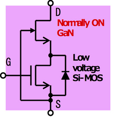
Figure 2: Cascode Structure of Normally On GaN with Low Voltage Si-MOS for pseudo-Normally Off Operation
The introduction of GaN devices opened to the idea of fast switching and more efficient power supply circuit design. Normally-on conventional GaN with I-V characteristics as shown in Figure 1 were initially developed. However, commercialization of this first generation GaN transistor was almost impossible due to an unwanted characteristic of the device during operation. A conventional GaN transistor operates in a normally-on condition where the device does not shut down even when there is no gate voltage applied. This raised safety concerns from the design engineers. Normally-on GaN requires a negative voltage to switch to an OFF state. With few options, manufacturers developed a countermeasure to transform normally-on GaN transistors to normally-off in order to enable the use of GaN in power circuits. This countermeasure is in the form of a cascode structure, as shown in Figure 2, where a standard low voltage Si-MOS with a normally-on GaN is packed into a module or multi-chip to achieve a pseudo-normally-off operation.
C;lick image to enalrge
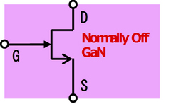
Figure 3(a): Single Normally Off GIT GaN Device
Panasonic, on the other hand, has a different story to tell. Using its novel Gate-Injection Transistor (GIT) technology fabricated on a Si substrate as shown in Figure 3, The companyc was able to develop a true normally-off GaN that does not need an additional Si-MOS or cascode module to complicate the device structure. Panasonic was able to develop a single GaN transistor with a very high reliability in a single package.
Click image to enlarge
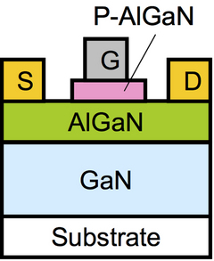
Figure 3(b): P-type AlGaN for Gate Electrode in Normally OFF GIT GaN Structure
Click image to enlarge
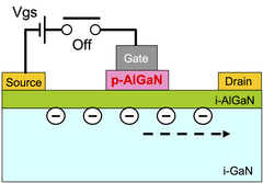
Figure 4(a): Electron Depleted in AlGaN/GaN Interface during Zero Bias
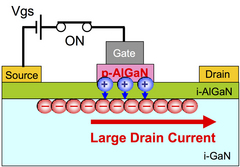
The GIT structure employs P-type AlGaN as the gate electrode. At zero gate-source voltage bias, the electrons at the channel deplete in AlGaN/GaN interface as shown in Figure 4(a). Drain current cannot flow in the transistor when there is no gate-source voltage injected. This shows a typical characteristic of normally-off operation, which is also similar to that of conventional Si-MOS. When a gate-source voltage that is higher than the threshold voltage is applied as shown in Figure 4(b), holes from the P-type AlGaN are injected into the channel by conductivity modulation. This generates an equivalent amount of electrons in the channel. The generated electrons that flow into the drain electrode increase the drain current. Since the effective mass of holes is 100 times larger than that of electron, the injected holes stay around the gate and allow electrons to increase to approximately 100 times of their normal amount. By this phenomenon, the resistance of the transistor drops dramatically.
These high mobility electrons that occur between the interface of AlGaN and GaN contribute also to the high switching speed. Therefore, by using a P-type AlGaN gate of GIT and by taking advantage of the conductivity modulation through holes injection from the gate electrode, a genuine normally-off operation is achieved and on-state resistance is reduced dramatically.
The earlier adoption of GaN transistor was mainly for low-voltage applications. It was almost impossible to adopt GaN transistor to high voltage application because of a GaN device natural phenomenon called ‘current collapse’, which occurs when the GaN on-resistance increases during the application of high voltage to the device. This is believed to be caused by trapped electrons in a high-electric field. However, the detailed mechanism that causes current collapse is still unknown and is still in the infancy of research.
Click image to enlarge
Figure 4(b): Conductivity Modulation when VGS>Vth
Click image to enlarge
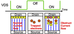
Figure 5: GaN Electron Trapping during On/Off Switching Leading to Current Collapse
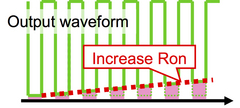
Current collapse can be illustrated in switching cycle using Figure 5. During the first ON state of the GaN device, the current flows normally after the formation of the channel. When the device is turned OFF in the next state, some electrons remain trapped in the channel hereby creating ‘trapped electrons’ that would eventually obstruct the smooth current flow. During this phenomenon, on-resistance increases continuously as the power device keeps on switching ON and OFF as shown in Figure 6. This phenomenon gives rise to the term of dynamic on-resistance or transient on-resistance. Electron trapping occurs at the interface between GaN and AlGaN when high voltage is applied. The increased amount of electron depends on electric field at the edge of the drain-gate side. The increase of on-resistance can degrade the efficiency of application, heat up the device and finally destroy the device irreversibly. This poses high safety risk on high voltage applications.
Click image to enlarge
Figure 6: Increasing Ron during the Current Collapse of Conventional GaN
To prevent current collapse and to ensure safety operations of GaN at high voltages, Panasonic uses novel technology to decrease the trap density by modifying the fabrication process. Moreover, crystalline quality of GaN is improved and a transistor structure that could reduce the electric field is adopted. As shown in Figure 7, the normally-off GIT GaN is tested up to 800V. Tests show that even at 800V the functions of the device was not degraded and the on-resistance did not increase unlike the conventional GaN structure. This is tantamount to a Current Collapse Free GaN transistor. This makes the Panasonic GaN suitable to use in continuous worry-free operation even at high voltage applications.
The lateral structure of the GIT also provides some advantages for high speed switching owing to the lower parasitic capacitance of the structure than that in conventional Si-based power transistors with the vertical structures. RonQg (Ron: on-state resistance, Qg: gate charge) is a figure-of-merit for high speed switching. The fabricated normally-off GIT GaN exhibits low RonQg of 715mΩnC, which is one thirteenth lower than that of the state-of-the-art Si MOS transistors. This only shows that the potential of the lateral structure is superior. The device potential is demonstrated in a 1MHz operation of resonant LLC DC-DC converters at high efficiency over 96% (1kW output). This demonstration indicates that the presented GIT on Si can be used for practical systems, free from the operation failure. Moreover, due to the similarity of operation as Si-MOS, this know-how can be applied easily when using normally-off GIT GaN.
With its novel technologies, Panasonic is able to offer high reliability and safety GaN transistor with a true normally-off and a current collapse free even at high voltages. Panasonic GaN transistor is the first in the world to be able to achieve stable operations up to 800V with the suppression of the increase of on-resistance during continuous switching operation. Panasonic GaN is expected to enhance power density and more energy savings of power supply and power management systems through more efficient and faster operations.


