Author:
Anup Bhalla, UnitedSiC
Date
03/11/2019
 PDF
PDF
Click image to enlarge
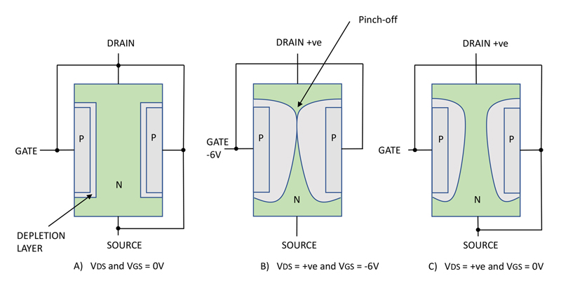
Figure 1. Basic JFET operation
Many think that Shockley invented the ‘transistor’, which he announced at a press conference on July 4th 1951. His Bipolar Junction Transistor (BJT) was certainly a momentous achievement, with the basic design still surviving today. Shockley, however, also had ideas about transistors using an electric field rather than current to control conduction as far back as 1939, but dropped the line of research after finding that Julius Edgar Lilienfeld had filed a patent for a Field Effect Transistor (FET) nearly 15 years previously in 1925. Colleagues tried to work around the patent but Shockley fell out with them and went his own way, working on BJTs instead. Lilienfeld’s patent for a FET was purely theoretical as there was no technology to fabricate such a device but the principle of an almost like-for-like replacement of the vacuum tube stood.
The FET or Junction Field Effect Transistor (JFET), in its simplest form, therefore has a long history. Despite a reputation for being outmoded, its modern-day incarnation in Silicon Carbide (SiC) technology is at the forefront of performance in switching circuits as a ‘cascode’ with a co-packaged MOSFET and, as a stand-alone device, has important applications in circuit protection and linear power circuits such as audio amplifiers and electronic loads.
JFET basics
Let’s backtrack a little and look at the basic principle of how a JFET operates.
From Figure 1, one can see that the JFET has two P-N junctions formed between the two gate connections and the drain-source channel. When there is no gate voltage, conduction can occur through the lightly doped N-type drift layer between drain and source, actually in either direction, depending on the polarity of the drain voltage. JFETs are ‘unipolar’ devices which means that current flows due to majority carriers, that is, electrons for the more common N (depletion mode) types. P-N junctions naturally form a separating ‘depletion’ layer which has no carriers and is therefore insulating. With no gate voltage, the depletion layer is relatively small and does not block the channel Figure 1A. If a negative bias -VGSis applied to the gate with respect to the source, the depletion layer widens progressively until at about -6 V ‘pinch-off’ occurs and the channel stops conducting. Figure 1B. With VGS = 0, an applied drain-source voltage VDSdoes cause the depletion layer to thicken towards the drain as shown in Figure 1C. This is because VDSadds to VGSreverse bias along the length of the channel and is in total higher nearer the drain end. This effect produces a natural ‘pinch-off’ with high drain currents producing a high voltage drop across the channel, usefully limiting current. A small positive bias can be applied to the gate to counter the effect and reduce the depletion layer further in the conducting state for lowest RDS(on).A positive VGSdoes however forward bias the gate-channel P-N junction for VGS>2.5V, so gate current can flow in this case and would require a series limiting resistor. Normally-on JFETs are usually operated with VGS= 0 for conduction.
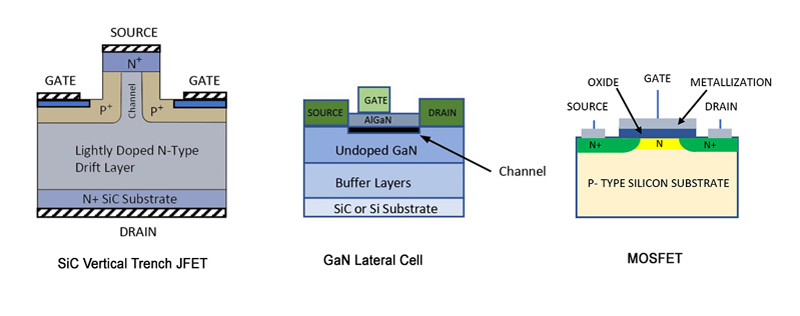
In a typical application, gate voltage is at zero or reverse biased so gate current is in the order of nano-amps. Gate charge is low due to the generally low device capacitances and when a JFET is implemented in wide band-gap SiC technology, the advantages of very high temperature operation, ultra-low RDS(on)and high frequency/low switching loss are available. Figure 2 shows SiC JFET vertical trench construction from UnitedSiC compared with a typical Gallium Arsenide (GaN) HEMT cell and a Si-MOSFET. Note the absence of any fragile gate oxide in the JFET.
Click image to enlarge
Figure 2. JFET, GaN HEMT cell and Si-MOSFET typical construction
SiC JFETs in cascodes
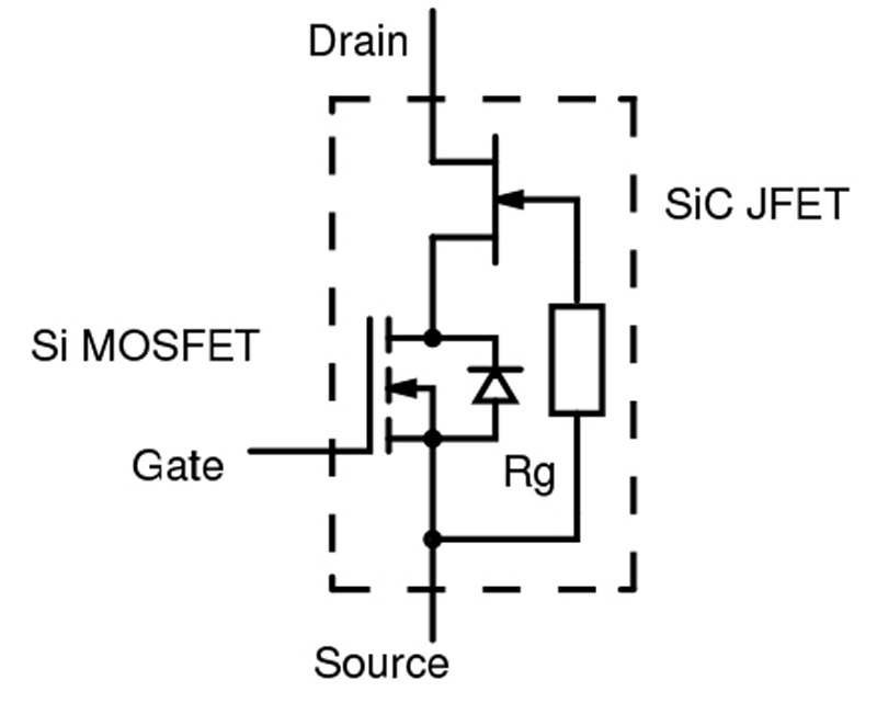
Although a device that is normally-ON with no gate voltage and which requires a negative value to be off is inconvenient in some applications, such as in switched mode power supplies, there are areas where it is a positive advantage. For example, when a SiC JFET is combined with a low voltage Si-MOSFET as in Figure 3, it becomes a ‘cascode’. In this arrangement, with a positive gate voltage, the MOSFET is on, pulling the JFET source to 0 V setting it on with its gate at 0 V. When the MOSFET gate is at 0 V, its drain rises in voltage, reverse biasing the JFET gate-source turning it off. The MOSFET drain only rises to around 10 V so can be a low voltage type with very low RDS(on), insignificant compared with the JFET. We now have a normally-OFF device with an easy gate drive, high voltage and temperature rating and with a bonus that the ‘Miller’ capacitance, which slows MOSFETs for example, is effectively absent. The SiC JFET has its natural current limiting due to the ‘pinch-off’ effect and is rated for high avalanche energies. For higher voltages, ‘supercascodes’ with further series JFETs give ratings up to several kV.
Click image to enlarge
Figure 3. The JFET in a ‘cascode’ with a Si-MOSFET
Current limiters and isolators
Another major JFET application area is in circuit protection where connections need to be isolated or current-limited. Normally-ON devices here may actually be preferred, with an active gate drive needed only when a fault is detected. SiC JFETS are an excellent choice - their very low on-resistance gives little power loss in normal operation and they can be chosen so that their natural saturation current is the circuit limit. This avoids the need for a separate lossy or expensive current sensing element such as a resistor or Hall effect device. The saturation current is also quite constant with drain voltage unlike Si-MOSFETs for example, keeping package dissipation more easily within limits. The saturation current has a negative temperature coefficient with SiC JFETs due to decreased electron mobility, again helping with power dissipation. Of course, the natural ruggedness of SiC is an advantage under the possibly unknown stress conditions of overloads. Peak junction temperatures have been recorded at 625°C with United SIC devices without failure for example and the excellent avalanche capability gives immunity to system overvoltages.
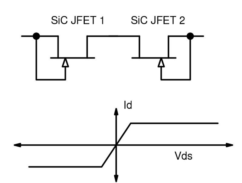
It’s difficult to imagine a simpler two-terminal bi-directional current limiter than two SiC JFETs in series, as shown in Figure 4, requiring no external power source with the circuit current limit set at the JFET saturation current.
Click image to enlarge
Figure 4. A simple bi-directional current limiter
When isolation of a circuit is required under fault conditions,mechanical circuit breakerscan be too slow andcumbersome while electronic breakers typically using IGBTs or MOSFETs are complex requiring auxiliary power rails. JFETs can be configured, with a little extra circuitry, as true, self-powered, two-terminal isolators with all sensing internal to the circuit with all the robustness you expect when fabricated in SiC technology.
SiC in its active mode
When used as controlled current limiters such as in electronic loads or in ‘linear’ applications such as audio amplifiers, SiC JFETs score points again: the transconductance of SiC devices has a negative temperature coefficient compared with other technologies[1], so less drain current is available at a given gate-source voltage as temperature increases. This effect prevents a common problem in linear applications using MOSFETs for example, where their positive temperature coefficient of gate voltage with temperature can cause current ‘crowding’ and hotspots leading to thermal runaway and device failure. This occurs even when the device seems to be working within its Forward Safe Operating Area (FSOA). Figure 5 shows the comparison between the temperature effects on drain current with gate voltage for SiC JFETS from UnitedSiC and a common SiC MOSFET.

Click image to enlarge
Figure 5. SiC JFET and SiC MOSFET opposite transconductance temperature coefficients.
Julius Edgar Lilienfeld may be largely forgotten today, but his legacy continues with SiC JFETS contributing to state-of-the-art switching performance and near ideal current limiting and protection. He also patented the electrolytic capacitor, but that’s another story…
UnitedSiC