High-voltage IGBT-modules usually consist of two types of IC, an IGBT for the transistor and a diode for the freewheeling functionality. A device that combines both functions in a single die is known as a reverse conducting IGBT (RC-IGBT). These modules exhibit a lower thermal resistance when compared to an IGBT of same footprint as the number of active die effectively increases. While the maximum junction temperature remains the same, greater current can be handled.
The gate terminal of the RC-IGBT can be used to control the diode; these devices are known as Reverse Conducting IGBT with Diode Control (RCDC). The RCDC characteristics in the forward conduction (IGBT) mode are similar to trench-field stop technology. Controllability during the reverse conduction (diode) mode by a dedicated gate drive scheme allows for further minimization of the dynamic losses during both IGBT turn on and diode turn off.
Chip design
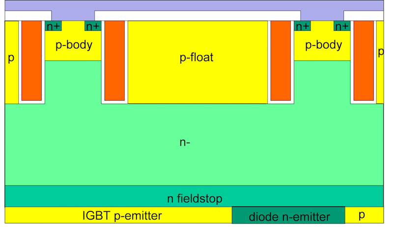
Infineon’s commercially available 6.5 kV IGBT3 trench technology has been modified to incorporate the diode function into the IGBT chip. The chip area exhibiting p-emitter portions on the backside serves as the “IGBT” as the electrons injected through the open MOS-channel cause electron–hole plasma during the IGBT mode. The chip area exhibiting n-emitter portions on the backside serves as the “diode” as holes injected from the front side p-doped silicon areas cause electron injection from the backside n-emitter regions (see Figure 1a).
Click image to enlarge
Figure 1: a) Schematic of the RCDC device
If the pitch of the alternating p- and n-emitter areas on the backside is sufficiently small with respect to the vertical dimensions of the device, one silicon volume serves both as diode and IGBT regions depending on the current flow direction in the RCDC chip. While the complete silicon area is used in IGBT mode, only part of it is used during diode mode. Additional continuous p-emitter areas on the backside overcome the snap-back behavior of the IGBT output characteristic.
The frontside p-doped silicon areas are designed with a minimum amount of highly doped anti-latch-up regions, maintaining the excellent overcurrent turn-off capability of IGBT3, in order to ensure a balanced carrier concentration and reverse recovery charge in diode mode without the use of any charge carrier lifetime control means.
Gate-controllability during diode mode
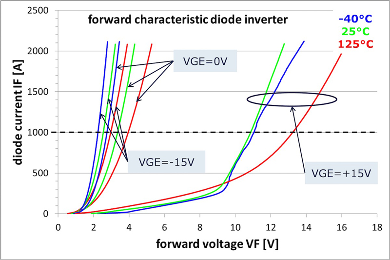
During the reverse conduction mode, the applied gate voltage (VGE) causes a varying p-emitter efficiency that is reflected in the slope of the diode forward characteristics. For gate voltages above the IGBT threshold, the front side p-emitter areas are bypassed by the open MOS electron channels. The current flowing is considered to be “quasi-unipolar”; an accumulation of holes in the drift region close to the gate trench occurs for negative gate voltages.
The accumulated holes and the optionally connected floating p-regions act as an additional hole source and thus increase the p-emitter efficiency. The resulting electron-hole plasma during diode mode is assessed by device simulation for VGE of -15, 0, +15 V (see Figure 1b). For a gate voltage below the IGBT threshold, the RCDC device is capable of forward blocking. Therefore, such a gate voltage can be used continuously during reverse conduction and blocking.

Click image to enlarge
Figure 1: b) Simulated carrier concentration of the RCDC in diode conduction mode along a vertical cut through a backside region with n-emitter for different gate voltages at Tj=125°C
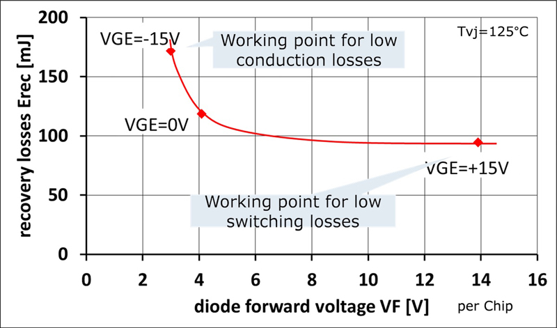
In Figure 1c the trade-off curve of the RCDC chip in diode mode is shown. The free parameter of this trade-off curve is the voltage at the RCDC gate terminal. The diode can be driven to different working points and, by applying a low gate voltage, low conduction losses can be enforced. By raising the gate voltage to +15 V, the diode can be prepared for turn-off with low switching losses. To combine both low on-state and low switching losses, a smart gate voltage pattern can be applied.
Click image to enlarge
Figure 1: c) Trade-off curve of the RCDC chip in diode mode with operation points for low conduction or low switching losses.
Module design and thermal behavior
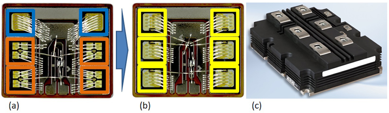
High voltage IGBT modules usually offer a 2:1 ratio of silicon areas for IGBT and diode die (see Figure 2a). The substitution of spatially separated IGBT and diode dies by RCDC chips allows for the integration of the RCDC technology into well-established industrial packages without changing the pinning of the module. This approach increases the silicon area used in IGBT mode by 50% while retaining the same footprints as shown in Figure 2b. Moreover, the effective diode area is increased by a factor of approximately 2 as each die is active during the freewheeling state. The new RCDC-module (FZ1000R65KR3) with a footprint of 140×190mm is rated with a nominal current of 1000 A (see Figure 2c).
Click image to enlarge
Figure 2: a) Commonly used IGBT (marked orange) and diode (blue) die combination
b) RCDC (yellow) assembly with same substrate layout
c) Well-established 190×140mm² industrial housing with high insulation capability
A general description of the module thermal behavior is described by a matrix representation
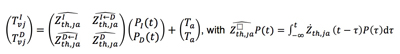
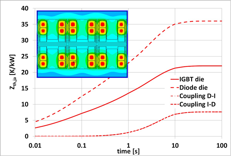
A common IGBT module supplies a combination of spatially separated IGBT and diode die on one base plate. The structure of the Zth,ja curves for the main diagonals (representing the direct heat paths) are different to the coupling terms (off-diagonals) due to their time-lag (see Figure 3a). On the contrary, the structure and absolute values of all Zth,ja curves are similar for an RCDC module as the heat loss is generated in the same piece of silicon which does not offer time delays in the cross coupling as shown in Figure 3b. A further simplification is possible for the RCDC module dealing with only one virtual junction temperature (Tvj) for transistor and diode action in one die. Thus, the matrix representation can be reduced to
Click image to enlarge
Figure 3a: Zth,ja for the different heat paths including the thermal cross-coupling - Standard IGBT module

Click image to enlarge
Figure 3b: Zth,ja for the different heat paths including the thermal cross-coupling
RCDC. Insets: simulated temperature distribution in the RCDC and IGBT module having the heat loss applied to the IGBTs. Model heat sink: 65 µm thermal grease with thermal conductivity of 1 W/mK, 3mm Aluminum heat sink with a heat transfer coefficient of 8000 W/m²K.
when appropriately averaging the single Zth,ja curves. This simplification appears to have an acceptable accuracy as the temperature distribution inside a module as well as on a single chip may significantly exceed the calculated differences.
The location of the virtual junction in an RCDC has to be carefully discussed. The RCDC-diode has its virtual temperature relevant pn-junction on the frontside as in a standard diode.
In a standard IGBT, the backside pn-junction offers the temperature dependent diffusion voltage used for sensing Tvj. For an RCDC-chip, this pn-junction is locally shortened by the additional n-short regions. The Zth curves for IGBT and diode mode of the RCDC refer to the die’s frontside temperature due to heating the same piece of silicon.
When comparing the benefits of RCDC-technology this has to be taken into account, especially when considering the IGBT operation mode. However, when calculating the power cycling capability, no differences are expected as the assembly technology has not changed and the PC reliability curves are valid for the common diode die with the pn-junction on their frontside.
Electrical behavior
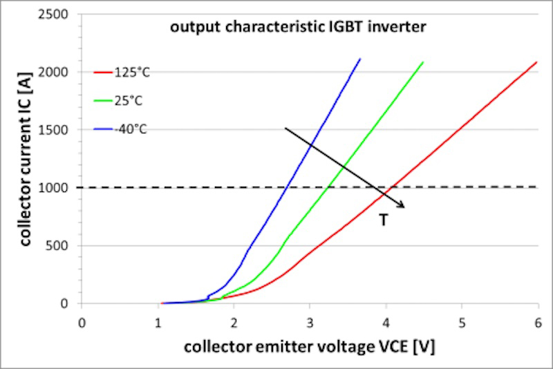
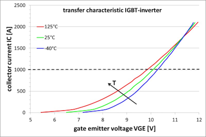
The IGBT output and transfer characteristics are shown in Figures 4a and 4b. The diode characteristic depends on the gate voltage actually applied to the module and can be seen in Figure 4c. This is a remarkable feature of the RCDC as it allows control of the on-state voltage but requires dedicated current direction detection during inverter operation.
Click image to enlarge
Figure 4a: Measured characteristics of the FZ1000R65KR3 - Output characteristics in IGBT mode
Click image to enlarge
Figure 4b: Measured characteristics of the FZ1000R65KR3 - Transfer characteristics in IGBT modeb) Transfer characteristics in IGBT mode
Click image to enlarge
Figure 4c: Measured characteristics of the FZ1000R65KR3 - Forward characteristics in diode mode
Gate-control of the RCDC
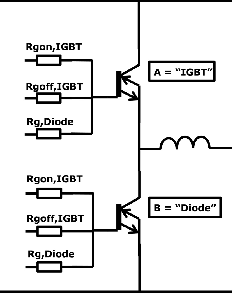
A schematic of a gate control pattern enabling the combination of lowest on-state and switching losses in a half-bridge configuration is shown in Figure 5a. Applying a gate voltage step to the RCDC in diode conduction mode shortly before commutation reduces the switching losses by sweeping out the stored charge carriers just before the turn on of the corresponding IGBT. This is referred to as the desaturation of the RCDC in diode mode. With this approach, the reverse recovery current peak (and therefore the switching losses) can be significantly reduced.
Click image to enlarge
Figure 5: a) Half-bridge configuration, module “A” in IGBT and module “B” in diode mode
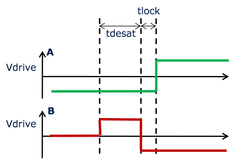
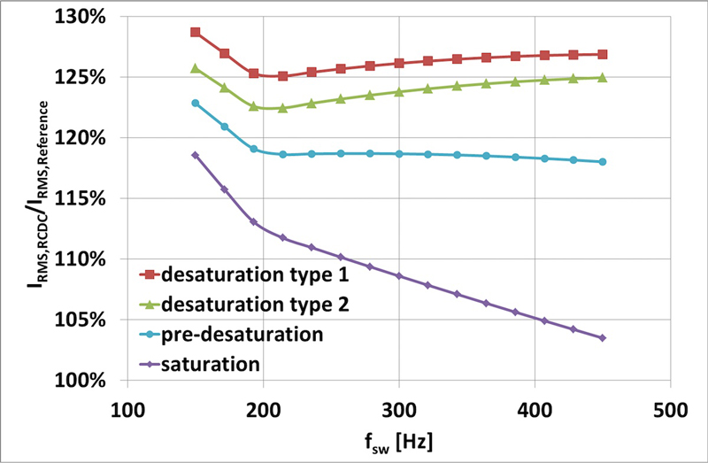
Essential desaturation parameters are the desaturation duration (tdesat) and the locking time (tlock) that avoids the occurrence of a phase leg short circuit. A variant of the gate control is the application of a gate-voltage of zero volts; The RCDC-diode conducts in a “pre-desaturated” stage. With this method, similar or lower dynamic losses can be achieved at shorter desaturation times.
Four operation modes for the RCDC in diode mode are specified:
VGE=-15V, no desaturation pulse: lowest conduction losses, but high switching losses due to highly saturated diode
VGE=-15V, with desaturation pulse: low conduction losses and low switching losses due to desaturation of the diode by tdesat before recovery (see Figure 5b). This desaturation mode is referred to as type 1 desaturation.

Click image tp enlarge
Figure 5: b) Gate control pattern with desaturation pulse applied to module “B” in diode mode
VGE= 0V, no desaturation pulse: higher conduction losses but lower switching losses compared to 1) due to less saturation of the diode (referred to as pre-desaturation)
VGE= 0V, with desaturation pulse: Due to 0V control, less charge has to be removed during desaturation time leading to shortest possible tdesat pulses (see Figure 5c). This desaturation mode is referred to as type 2 desaturation.
Click image to enlarge
Figure 5: c) Gate control pattern with a pre-desaturated module in diode mode
Loss comparison and output current benefit
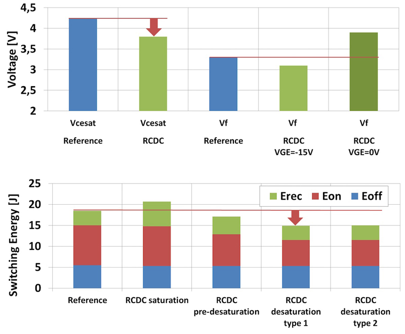
Figures 6a and 6b compare the sources of electrical losses in an RCDC module with an appropriate reference, Infineon’s FZ750R65KE3 rated at 1000 A. A reduction of the static and dynamic losses is possible if using the diode control patterns. The reduced losses together with the better heat spreading in a RCDC module result in an increased inverter output power while using the same heat sink. The RCDC also benefits from reduced Tvj ripple.
Click image to enlarge
Figure 6: a) Comparison of static losses (described by forward voltage drops at IC=1000A) and dynamic losses at Tvj=125°. Reference module is Infineon’s FZ750R65KE3
Click image to enlarge
Figure 6: b) Inverter gain by replacing the reference by a RCDC module taking into account the different operation modes of the diode.


