Author:
Victor Khasiev, Analog Devices, Inc.
Date
07/02/2020
 PDF
PDF
Click image to enlarge
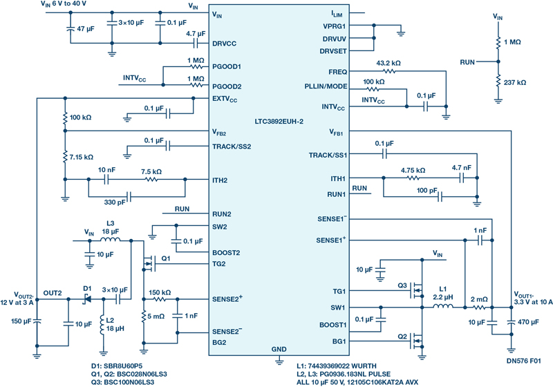
Figure 1. Electrical schematic of LTC3892 in SEPIC and buck application
Each new chip used in an industrial or automotive setting must be qualified via extensive testing before it can be utilized in demanding environments. Implementing a different IC for each application is time consuming and cost prohibitive. It is far better to have a tested and verified IC on the shelf that can be used in multiple topologies, which allows it to be reused across a variety of applications. As an example, this article will show how to use the LTC3892 step-down controller for SEPIC (step-up and down) and boost applications.
Circuit Description and Functionality
The LTC3892 is designed as a dual output synchronous buck controller with input-output voltage range 4.5 V to 60 V—covering the requirements for most automotive and industrial applications. In these environments, the voltage input to the converter can vary significantly, such as those resulting from cold cranking and load dumps in automotive applications, or brownouts and voltage spikes in industrial systems when plant machinery is turned off and on. The native step-down topology of the LTC3892 can not regulate output voltages when the input drops below the output, but a SEPIC topology can.
Figure 1 shows a SEPIC solution that supports two outputs: VOUT1 is 3.3 V at 10 A and VOUT2 is 12 V at 3 A. The input voltage range is 6 V to 40 V. VOUT1 is implemented as a straightforward step-down converter with a power train including L1, Q1, and Q2. To reduce number of components, the VPRG1 pin is connected to GND, internally programming VOUT1 to 3.3 V.
The second output of the LTC3892 is a SEPIC converter. The SEPIC powertrain includes L2, L3, Q3, and D1. A noncoupled SEPIC, with two discrete inductors, is employed here, expanding the range of the available inductors. This is an important consideration for cost-sensitive devices.
Click image to enlarge
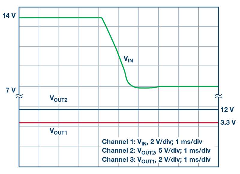
Figure 2. Shows a cranking event. The rail voltage drops from 14 V to 7 V, but both VOUT1 and VOUT2 remain in regulation
Click image to enlarge
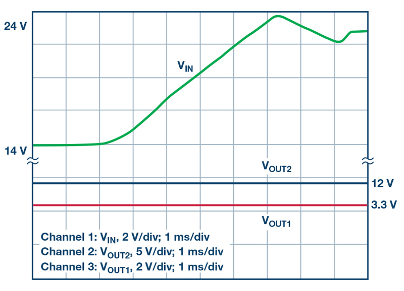
Figure 3. Load dump event. The rail voltage rises from 14 V to 24 V. However, both VOUT1 and VOUT2 stay in regulation
Figure 2 shows how the converter functions when faced with voltage drops, such as during cold cranking. The rail voltage VIN drops far below nominal 12 V, but both VOUT1 and VOUT2 remain in regulation, providing a stable power supply to the critical loads. Figure 3 shows how the converter functions when experiencing voltage spikes, such as load dumps. VOUT1 and VOUT2 remain regulated, even as VIN flies far above the nominal 12 Vinput.
Figure 4 is the demonstration circuit DC2727A, a dual output converter described herein. The SEPIC portion of the DC2727A can be easily rewired to a boost topology by removing one inductor L2 and replacing the second L3 to an appropriate boost choke.
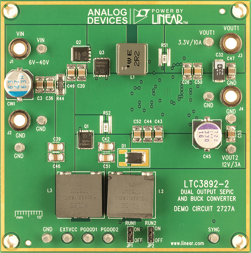
Click image to enlarge
Figure 4. Demonstration circuit DC2727A. The LTC3892 controls two outputs: a noncoupled SEPIC and a step-down converter
Conclusion
The LTC3892 is a flexible controller that can serve a variety of dc-to-dc converter needs in automotive and industrial environments. Although it is primarily designed for employment in synchronous buck converters, it can also be used in SEPIC and boost converter applications, which simplifies the qualification testing process when these topologies are needed.