Author:
Jennifer Joseph, Applications Engineering Manager, ON Semiconductor
Date
04/09/2018
 PDF
PDF
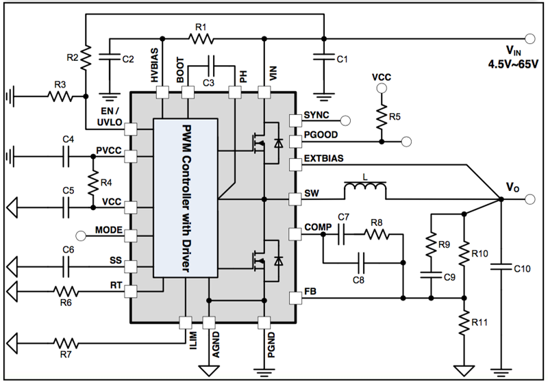
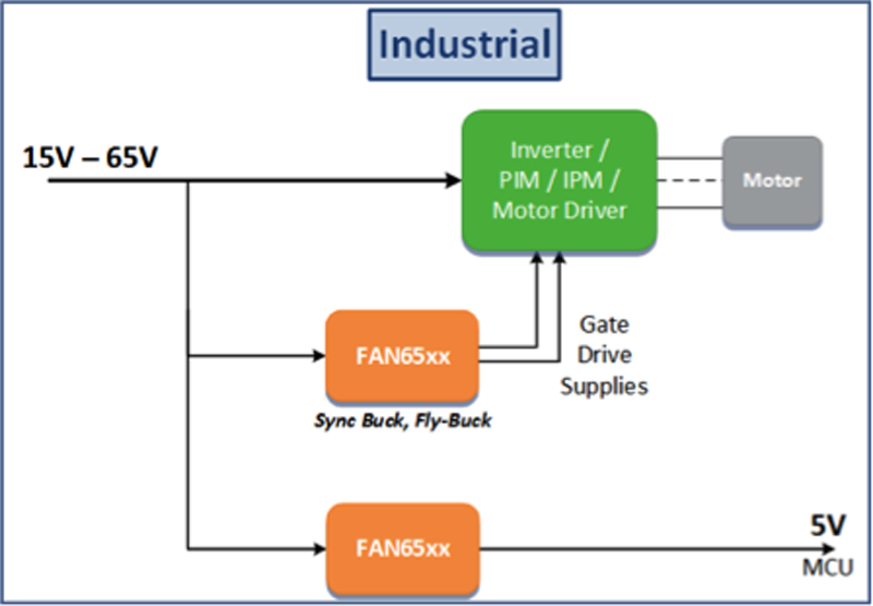
Figure 1. The FAN6500XX in a typical application
Integration is fundamental to solid-state electronics — the ability to bring together similar and complementary functions into a single device drives the entire industry. When coupled with developments in packaging, wafer handling and lithography, feature density continues to rise, delivering more efficient solutions both in terms of physical size and power.
Power density is an ever-present challenge for product developers, the demand for higher current at various voltages, that are often much lower than the system bus, is creating demand for smaller buck regulators that can convert voltages as high 48 V down to 1 V with multiple Amps in a single stage, allowing them to be applied closer to the point of load and still deliver efficiencies over 95%.
The combination of high levels of integration and power conversion are not traditionally good bedfellows as, normally, the processes used for both are not completely compatible. In some cases the inevitable compromises can be tolerated, such as in DC/DC regulators that deliver low levels of power from a relatively narrow input voltage range, or where poor power efficiency can be ignored. Unfortunately for system developers, these kinds of compromises are becoming less tolerable.
A small number of power regulators now offer good levels of integration, but they are generally poor on performance and efficiency. In an increasing number of applications, where compromises are less tolerable, the level of integration is often limited to a controller and low-side/high-side drivers for external MOSFETs. However, the ideal solution would see all of the buck converter functionality integrated into a single, small and efficient device, bringing together the controller, driver and MOSFETs to provide greater overall system benefits.
Better together
There are many reasons why integration makes sense. In a digital or mixed-signal solution, such as a microcontroller, integration consolidates a number of functions that would normally be needed in a range of applications. Putting these functions and feature sets together in a single device results in a solution that appeals to a reasonably large number of manufacturers while typically lowering the overall BOM cost. In this case, integration is enabled by developments in the semiconductor fabrication processes used.
In a power device, integration can also deliver cost benefits but in a more impactful way; a closer integration between the main components used in buck conversion, for example, can deliver direct efficiency gains, which not only translates into lower BOM cost, but also system power savings. Often, as a result of higher efficiencies, manufacturers can also achieve lower overall system cooling requirements. This can result in a direct saving in the total cost of ownership in a growing number of applications, such as telecommunications and networking equipment, base stations, industrial automation (including robotics), home appliances and power tools, vending, gaming and financial machines (ATMs), and the power supplies used to charge our portable devices.
Multichip module
Bringing multiple components together in a single package can be achieved by one of the two approaches; multi-chip-modules (MCM) or monolithic. MCM comes with performance improvements, miniaturization and much faster introduction of the product into the market, compared to integrating all the desired functions on a single monolithic chip. For a component manufacturer such as ON Semiconductor, having access to the most suitable technology allows for an optimized approach to developing a multichip module.
At a high level, there are three key functions in a synchronous buck regulator topology, the controller, the Gate driver(s) and the switching power MOSFETs. There are examples of devices that successfully integrate the controller and driver(s), for use with external MOSFETs, but few that are able to integrate all three functions in a single device that offers appreciable advantages to system engineers.
The FAN6500XX family of voltage mode synchronous buck regulators offer this level of integration. Taking a purposeful approach to integration means every element is designed and optimized for the task, resulting in a multichip module that combines class-leading current output with a level of performance that is difficult to achieve using discrete components.
The family currently includes three devices, differentiated by their current output of 6A, 8A or 10A. Pin-compatibility is maintained between all members, packaged in a space-saving 6 mm x 6 mm PQFN profile. Consequently, OEMs can choose the most optimum device for their application even after the PCB design has been finalized. Figure 1 shows a functional diagram of the FAN6500XX in a typical application.
A major advantage of integrating the high- and low-side MOSFETs into the same package is the optimization of the drive strength to MOSFET load.In a conventional solution the MOSFETs are external and selected as per the output current requirements. Although this can be beneficial, when designing for the current required, it does present several disadvantages, that the MCM overcomes.
While the actual supply current that can be delivered will still be limited by the capacity of the integrated Gate driver(s), the main challenge with external MOSFETs comes with closing the control loop in terms of sensing the high-side current. This is a crucial part of the overall solution, as it provides regulation as well as over-current protection. With internal MOSFETs designed alongside the controller and driver means the temperature coefficients between all parts of the circuit are much more closely matched, delivering far greater accuracy. With a topology that uses external MOSFETs this close matching is lost, which can result in lower efficiency.
A further advantage of actually developing the components for a multichip solution is it allows for closer design optimization between the Gate driver and the MOSFETs. This means the slew rate of the driver can be tailored to the MOSFETs (in this case, ON Semiconductor’s PowerTrench MOSFET technology is used). This delivers lower switch node ringing and very less risk of shoot-through or cross –conduction. Reliability is also improved, as the modular approach means there is now only a single point of failure in the power supply design. The qualification process is implemented with the whole solution, rather than on bits and pieces, which paves way to less assumptions and thereby less risks.
Multimode operation
In addition to the advantages of high integration, the FAN6500XX family offers multiple operating modes for greater design flexibility. This includes CCM and DCM in both Master and Non-Master mode. The Mode pin on the device controls whether it operates in Pulse Modulation or Frequency Synchronization mode, which creates many design possibilities. Figure 2 A-C shows typical application examples for the FAN6500XX family.

Click image to enlarge
Figure 2 A-C. Design examples of how the FAN6500XX Family can be used to operate in either Forced CCM or DCM modes.
In Forced CCM mode, it remains in Continuous Conduction Mode with a fixed frequency, irrespective of the load conditions, delivering a low ripple output. If the device operates in DCM mode it will implement pulse skipping at light loads, and automatically switch to CCM mode when the inductor current is above 0A. Pulse skipping feature provides greater operating efficiency in applications with lighter loads or during standby periods.
When in Master mode operating in Frequency Synchronization, the device generates a clock signal that is 180° out of phase with its own clock, allowing multiple devices to be synchronized while keeping the input ripple to a minimum, leading to greater overall system efficiency.
Thermal management
The multichip module design allows the Source of the low-side MOSFET to be physically attached to a large Ground plane. This in turn creates an efficient thermal path to the inner layers of the PCB using vias. This design improves the module’s thermal characteristics further increasing overall efficiency.
The use of PowerTrench MOSFETs and a thermally enhanced compact 6 mm x 6 mm PQFN-35 package enables the FAN6500xx family to deliver high power density performance.
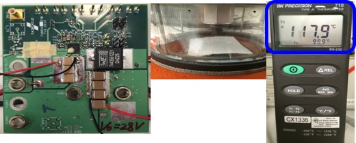
In Figure 3, the FAN65004B is used to build a 48 V input to 28 V output converter, at 5A output current.
· Case temperature thermo couple placed on high-side FET: (T1 = 117.9⁰C)
· Ambient temperature thermo couple placed on bottom: (T2(TA) = 98.9⁰C)
The solution delivers 140 W of output power at 97% efficiency with just 19˚C increase in temperature
Click image to enlarge
Figure 3. Example of the thermal efficiency of the FAN6500XX family
The FAN6500XX (FAN65004B, FAN65005A, FAN65008B) family of voltage mode synchronized buck regulators offer a complete solution in a single module, helping system engineers and power supply designers to achieve significantly greater power density for a broad range of applications. With a wide input voltage range of 4.5 V to 65 V, output voltages from 0.6 V to 55 V, and continuous current of 6 A to 10 A. The FAN6500XX family takes power density to industry leading levels of integration.
On Semiconductor