Optimizing Flying Capacitor Multilevel Converters for GaN Technology

Design Techniques and Real-World Implementations of GaN-Based Multilevel Converters
Introduction
Modern power systems demand higher efficiency, increased power density, and reduced electromagnetic interference (EMI)—all while adhering to shrinking size constraints. Among the converter topologies addressing these challenges, the Flying Capacitor Multilevel (FCML) converter stands out for its unique advantages. When combined with Gallium Nitride (GaN) power transistors, FCML converters offer an unprecedented level of performance, particularly in the realm of medium-voltage applications such as 48 V data center power delivery, battery management systems, and high-efficiency power factor correction (PFC) circuits.
This article explores the operating principles, device-level figures of merit, key design equations, gate drive strategies, and practical implementation details that make GaN-based FCML converters a compelling solution for next-generation power electronics.
Why Multilevel Conversion and Why Flying Capacitor?
Multilevel converters work by generating a stepped output voltage waveform, approximating a sinusoidal or reduced-ripple DC waveform using multiple lower-voltage transitions. This is particularly advantageous in medium- to high-voltage systems, where high switching speeds and reduced stress on components are crucial.
Among the available multilevel topologies—such as cascaded H-bridge (CHB) and modular multilevel converters (MMC)—the FCML stands out due to:
- Use of a single DC source, simplifying power delivery compared to MMC and CHB, which require isolated sources per level.
- Natural voltage self-balancing when using phase-shifted pulse-width modulation (PSPWM), reducing control complexity.
- Scalability to a higher number of levels without needing high-voltage switches.
GaN Technology Synergies with FCML Topology
The synergy between GaN devices and FCML topology is particularly strong for three primary reasons:
-
Voltage Step Reduction
The voltage across any single switch is reduced to:
allowing the use of lower-voltage-rated GaN FETs (e.g., 100 V or 200 V), which have significantly better performance metrics than their high-voltage counterparts. At the same time, lower voltage steps result in lower EMI generation.
Figure of Merit (FOM) Superiority
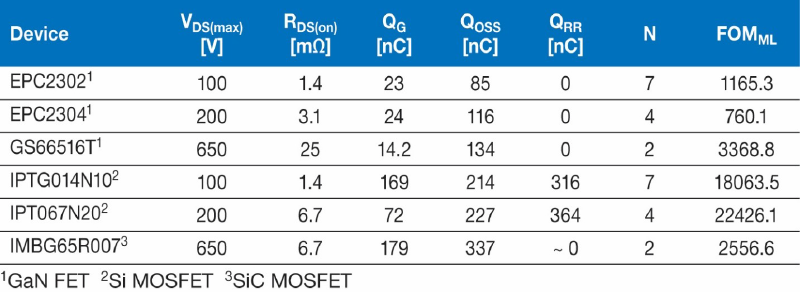
For hard-switching applications, three standard FOMs are used:
· FOM1: RDS(on) X QG – Conduction efficiency
· FOM2: RDS(on) X QOSS – Switching losses
· FOM3: RDS(on) X QRR – Reverse recovery loss (0 for GaN)
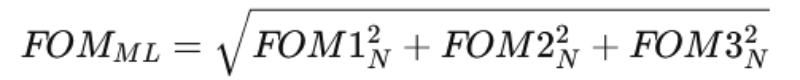
The composite multilevel figure of merit, FOMML, scales with the number of levels and is minimized for GaN:

Click image to enlarge
Table 1: Hard switching figure of merit for a multilevel converter with N levels
FCML Control and Capacitor Voltage Balancing
A distinguishing feature of FCML converters is their self-balancing behavior. Using PSPWM, the timing of adjacent switch cells is offset by a phase shift of:
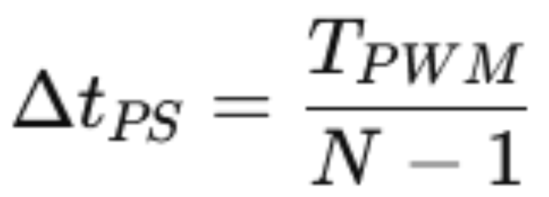
This ensures that each flying capacitor undergoes symmetrical charge and discharge cycles, maintaining voltage equilibrium across levels under steady-state operation.
While ideal PSPWM naturally balances capacitor voltages, real-world imperfections—like mismatched propagation delays in gate drivers—can introduce voltage drift. In such cases, active balancing methods dynamically adjust duty cycles based on real-time capacitor voltage feedback.
Flying Capacitor Sizing
Flying capacitors must be correctly sized to support load transients and voltage ripple requirements. The fundamental equation for determining the required capacitance is:
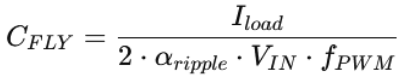
Where:
For GaN-based FCML converters operating at MHz frequencies, capacitor size and quantity can be reduced—although careful attention must be paid to derating due to DC bias and temperature, especially for ceramic types like X6S and X7T.
Inductor Design Benefits in Multilevel Topologies
FCML topologies significantly reduce the effective voltage and increase switching frequency seen by the inductor, resulting in drastically smaller required inductance:
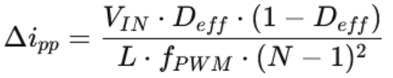
Thus, a 3-level FCML (N=3) enables up to 4× inductance reduction, while a 4-level topology can yield a 9× reduction.
This scaling is particularly useful in low-profile designs (e.g., laptop chargers, TV adapters), where inductor height and core volume are limiting constraints.
Gate Driving Challenges and Solutions
Problem: Floating Switch Nodes
Every GaN device in a multilevel converter (except the bottom switch) operates at a floating potential. This makes gate driving complex, as each gate driver must be referenced to its switch’s source potential.
Conventional Bootstrapping
Using diode-based bootstrapping cascades leads to insufficient gate voltages at higher levels due to:
- Cumulative forward voltage drops
- Overcharging due to GaN’s body diode conduction during dead time
Zener Clamp Bootstrap
A practical alternative involves clamping the bootstrap capacitor voltage with Zener diodes (e.g., 5.1 V, 5.7 V) to regulate gate voltages across stages. This achieves acceptable variation (±0.3 V), though it introduces higher power dissipation—up to 0.36 W in some designs.
Synchronous Bootstrap Circuit
For low-loss, high-efficiency systems, a synchronous GaN-based bootstrap offers superior performance. It uses low-current GaN FETs (e.g., EPC2038) to replace diodes in the charging path, ensuring:
- Gate drive voltages between 4.7 and 5.2 V
- Low dropout voltage
- Elimination of UVLO triggering
- Excellent scalability to >4 levels
This approach minimizes gate drive losses (as low as 65 mW at full load), preserving GaN’s efficiency edge.
Integrated 5 V to 5 V Isolated DC/DC Module
In recent years several manufacturers have introduced compact and cost-effective isolated DC-DC modules that are ideal for multilevel converters. These modules are isolated 5 V to 5 V converters with up to 1.5 W rating, contained in a 4 x 5 mm low profile package.
Compared to the bootstrap solutions discussed earlier, they offer a more tightly controlled supply for the gate driver, and they enable duty cycles from 0 to 100%.
Real-World FCML Implementations
1. Three-Level 48 V Buck Converter for Server Power Delivery
This implementation addresses the increasing power density requirements of 48 V power architectures in data centers. The three-level FCML topology enables a significant reduction in inductor size—down to 3.5 mm height—while maintaining thermal efficiency. The converter utilizes 40 V EPC2055 GaN FETs for the inner switches and a 100 V EPC2218 for the top-level switch to manage transient startup conditions. Operating at 400 kHz, the multilevel converter outperformed a two-phase interleaved buck design by achieving 1.2% higher efficiency and reducing thermal rise by over 10°C at a 12.5 A load. This configuration illustrates how FCML enables higher rack density, lowers cooling demands, and supports increased computational throughput in AI and cloud infrastructure.
2. 300 V Bi-Directional Buck-Boost Converter for Battery Interfaces
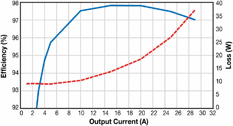
Designed for industrial systems and energy storage, this two-phase, three-level converter interfaces between a 200 V battery and a 40 V load. GaN FETs (200 V, 8 mΩ EPC2215) were configured in parallel to handle high currents, and the converter was designed to operate under 50% duty to simplify gate drive design. The architecture achieved over 97.8% efficiency at 20 A, while the compact layout and targeted thermal design allowed passive cooling with a small 50 × 30 mm heatsink. This implementation is ideal for regenerative braking, V2G applications, and bidirectional energy flow in renewables.
3. Four-Level Totem-Pole PFC for 3 kW AC-DC Conversion
A high-density PFC solution using a four-level FCML totem-pole topology was developed for telecom and industrial systems. EPC2215 GaN FETs were used in the high-frequency leg, while low RDS(on) silicon MOSFETs handled the low-frequency leg. The design achieved >99% efficiency across a 1–3 kW load range. With a 13.2 μH inductor built from four low-profile 3.3 μH windings, the system achieved a power density of 129 W/in³. The converter maintained THD below 3%, operated with minimal airflow (200 LFM), and showed excellent thermal stability, making it ideal for compact front-end power supplies.
Click image to enlarge
Figure 2: Measured efficiency (left axis) and power losses (right axis) with VOUT = 40 V and VIN = 200 V
Flying capacitor multilevel converters, when implemented with GaN transistors, offer a superior approach to achieving high-efficiency, high-density, and low-noise power conversion. Their natural compatibility with low-voltage GaN FETs, reduced passive component requirements, and flexibility across a range of applications—from data center power to EV subsystems—positioning FCML converters combined with GaN technology as a leading solution for future power systems.
With continuous innovation in GaN packaging, smart gate driving techniques, and advanced control algorithms, FCML-GaN architectures will play a central role in reshaping power delivery efficiency in high-performance electronics.