Optimizing high-volume power semiconductor test (Part 1)
Using a modern source measure unit (SMU) instrument can simplify issues
Configuring high volume test systems for power semiconductors requires balancing the need for high throughput with the need to ensure high measurement integrity. This article addresses some specific challenges of these types of testing applications and how the features and characteristics of modern source measure unit (SMU) instruments can simplify facing them.
Statistical Testing
Obviously, when experimental devices are being characterized individually in a bench-top environment in the lab, high testing throughput is not a priority but measurement integrity is. However, once sample testing is complete, the device enters the statistical sample-testing phase, where the number of devices tested and the volume generated usually requires the use of a much more automated process. Although there are several vendors of automated power device test systems, such systems are expensive and the scope of the tests they can perform is often limited.
In many cases, wide bandgap materials such as silicon carbide (SiC) or gallium nitride (GaN) are increasingly being used for these high power applications. These wide bandgap devices offer the promise of reduced weight, volume, and power consumption in many end-use applications because they can operate at higher temperatures, voltages, and frequencies with lower power loss than silicon devices.
Because devices fabricated with these newer materials exceed the performance capabilities of standard Si devices, they often require test engineers to revisit the test equipment and methods used in characterizing them. For example, typical drain leakage currents on a silicon carbide power FET might be less than one nano-amp, but an automated power device tester is often limited to hundreds of nano-amps or even micro-amp capability.
One solution is for the power device manufacturer to configure their own automated solutions using higher performance instrumentation, such as the latest high power SMU instruments, which now offer numerous features designed to simplify the development of automated systems, including built-in scripting capability, and virtual backplane capability for synchronizing multiple instruments for more complex solutions. Fortunately for system builders, software specifically designed to control and manage automated testers is readily available. For example, Keithley’s Automated Characterization Suite (ACS) software was specifically designed to manage data acquisition and data management across multiple devices undergoing multiple tests.
Long Term Life Testing
Once a designer is satisfied that a statistical sample of the devices perform as required, the next step is a production qualification run. From these wafers, a Long Term Life Test can be set up to validate the reliability of the devices under different conditions designed to emulate the real world. This is normally done in large parallel batches, with many devices installed in thermally controlled environments.
Many hundreds of devices are tested for hundreds or thousands of hours under various electrical and environmental stress conditions. In most cases, designers have specific conditions that they want life-tested, which make it essential that the test equipment be flexible and readily reconfigurable.
Creating and maintaining parallel test resources and monitoring and managing the masses of data acquired during this phase can easily become overwhelming. Typical parameters tested here include leakage current (IDSS and IGSS), ON resistance (RDS(ON)), and threshold voltage drift (delta VTH).
Production Testing
Production test includes wafer level tests such as die sort, known good die (KGD) testing, or wafer acceptance test. Testing modern power semiconductors in the production environment presents a variety of measurement challenges. And because wide bandgap devices are relatively new, the processes used in their fabrication are not yet fully mature, which can result in wider process variations. The combined effect can make testing very challenging, and often drives the need for higher levels of accuracy in order to gain insights into subtle process variations to improve processes and yields.
At the same time, the operating parameters of newer power semiconductor devices, whether they made from wide bandgap materials or traditional silicon, are being pushed to new extremes, including higher breakdown voltages, lower leakage currents, lower on resistances, and higher power levels. This means the test equipment must offer sufficient dynamic range and resolution to handle these parameters.
As always, test engineers are under relentless pressure to continue lowering the cost of test. This means that the test equipment must be capable of faster throughput while enabling higher yields and minimizing upfront capital investment.
The challenges of high-voltage test
High voltage device testing presents some significant challenges, especially the need to source high voltages and measure extremely low currents accurately. Figure 1 illustrates using a 20msec voltage pulse to test an IGBT. The first step is to charge the device to the rated test voltage as quickly as possible, then take the measurements as quickly as possible, and finally discharge as quickly as possible, then move on to the next test.
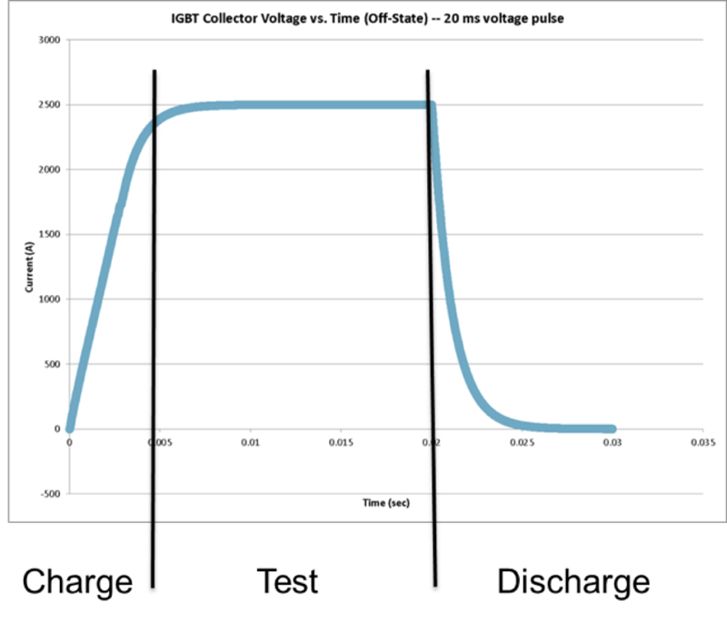
Clcik image to enlage
Figure 1. IGBT test with a 20msec voltage pulse
To maximize throughput during high voltage testing, a four-quadrant SMU instrument provides optimal performance. The diagram on the left half of Figure 2 illustrates an SMU instrument’s operating range; it can both source and sink both voltage and current, while simultaneously measuring voltage, current, or resistance.
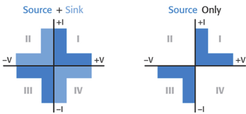
Clcik image to enlarge
Figure 2. SMU instrument vs. a traditional power supply
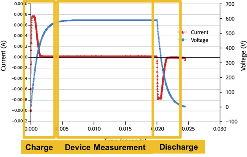
In addition, SMU instruments can be used as stand-alone constant voltage or constant current sources, as stand-alone voltmeters, ammeters, and ohmmeters, and as precision electronic loads. Their high performance architecture also allows using them as pulse generators, as waveform generators, and as automated current-voltage (I-V) characterization systems. The diagram in the right half of Figure 2 illustrates a traditional power supply, which can only source voltage or current. It cannot sink, which means the voltage pulse applied to the device will take much longer to discharge. In addition, it has very limited measurement resolution (often called “readback”), so a separate DMM is normally required to make measurements, which can further slow the testing process. Figure 3 illustrates the impact of an SMU instrument’s four-quadrant architecture on testing performance.
Clcik image to enlarge
Figure 3. The advantages offered by four-quadrant SMU instrument technology
The blue waveform represents the voltage pulse. The red waveform is the current that is flowing. During the charge phase, a high level of current forced into the device in order to reach the programmed voltage as quickly as possible. The current increases quickly in order to “push through” any impedance in the cabling and connectors. Once the voltage reaches its programed value and the total system capacitance is charged, the current drops to the level dictated by the device impedance, then measurement of the device is made.
The SMU instrument allows sourcing and measuring simultaneously, so the overall measurement time is minimized and sourcing and measurement are performed by the same instrument, which eliminates the delays involved in sending trigger signals to a separate measurement instrument.
Note how the current goes negative during the discharge phase—behavior made possible by the four-quadrant SMU instrument architecture. The SMU instrument is actually absorbing or sinking the current, discharging the device and system capacitance. All the charge is pulled from the device and cabling, very quickly pulling the voltage down to zero. A typical two-quadrant power supply can’t do this because it can’t sink current. Therefore, the device under test will take much longer to discharge if only a power supply is used. In this scenario, the discharge time depends on the impedance of the system itself (power supply output impedance, cabling, DUT, etc.).
In Figure 4, the discharge time of a power supply (left) is compared with that of an SMU instrument (right). In both cases, an oscilloscope captured the discharge curve of a 1000V capacitor. Although the discharge curves initially appear somewhat similar, note that the timescale for the power supply is 2 seconds per division, but the timescale for the SMU instrument is 2 milliseconds per division. The SMU instrument discharges more than 1000 times faster.
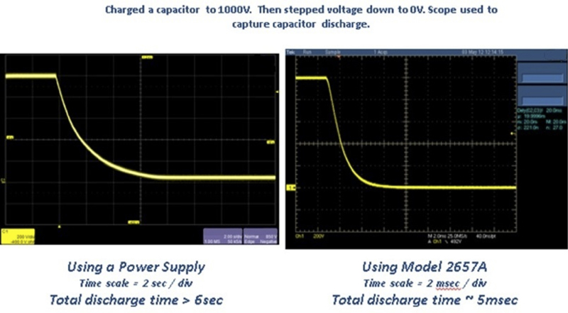
Clcik image to enlarge
Figure 4. Discharge time of a power supply vs. an SMU instrument
In Part 2 of this article we will explore the importance of choosing the right cabling to enhance test throughput and overall measurement quality.