Better components make for a better circuit
Poised to deliver incredible efficiency, safety, and convenience improvements across all market sectors and applications, the Internet of Things (IoT) is experiencing rapid and widespread growth. In fact, Gartner estimates that 20.8 billion IoT devices will be in active operation by 2020 [1].
IoT device designers are challenged to create miniature modules that use low amounts power, exhibit long lifetimes, and commonly measure physical conditions, such as temperature, humidity, and vibration, amongst others. To help designers satisfy the demands of this burgeoning industry, suppliers are creating whole new chipsets dedicated to addressing their specific electrical and mechanical requirements.
When designing IoT chipsets, suppliers focus an extreme amount of attention on power sources and power consumption. As, with the correct selection of ICs, IoT modules can exhibit active power consumption levels in the 6mA range and sleep mode power consumption levels around 1uA. Such low levels of power consumption allow some IoT modules to operate indefinitely, powered by energy harvesters rather than a battery or connections to an external power supply.
The ability to achieve such efficient IoT designs is largely determined by component selection, and specifically by a design’s power, input sensor, output matching, and timing block components.
Power Components
Both tantalum and ceramic capacitors are an excellent choice for IoT module power systems. Tantalum capacitors can provide extremely high capacitance values in compact, low profile packages and, as a result, can act as the energy storage source for energy harvesting powered modules. De-rating — or using a part with a higher rated voltage than the application voltage — plays a critical role in achieving such optimal performance by decreasing the leakage current of tantalum capacitors in an application.
Figure 1 shows the reduction of leakage current in tantalum capacitors as the ratio of applied voltage to rated voltage decreases. The greater the level of voltage de-rating, the lower the leakage current level in the application. For example, a part used at 50% of its rated voltage will have more than three times lower leakage levels than one used at 80%.
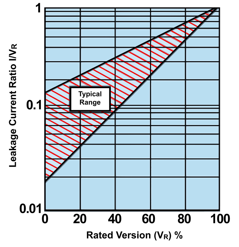
Click image to enlarge
Figure 1: Typical leakage current vs. applied voltage in tantalum capacitors
Ceramic capacitors, and especially X5R dielectrics, can also deliver high capacitance values in miniature case sizes, including ultra-small form factors, such as 0201 or 01005, which provide engineers with the critical space savings required to enable sleek, extra small, and easily portable IoT devices. Additionally, ceramic capacitor technology typically exhibits low ESR, which can be especially useful when creating filters to attenuate specific portions of the RF spectrum in an application.
Input sensors
Since IoT devices are used in such a wide range of application environments, designers commonly employ transient voltage and EMI protection in the modules. Multilayer varistors (MLVs) are multifunction components that provide designers with the ability to manage both transient voltage threats and EMI with a single component solution, saving both board space and BOM costs.
MLVs are fabricated using a ceramic sintering process that yields a structure of conductive ZnO grains surrounded by electrically insulating barriers, creating varistor-like behavior. The number of grain-boundary interfaces between conducting electrodes determines the breakdown voltage of the device. High voltage applications, such as AC line protection, require many grains between electrodes, while low voltage applications, such as low-core voltage ASICs, only require a few grains to establish the appropriate breakdown voltage.
MLVs are manufactured by mixing ceramic powder with an organic binder, casting the resulting slurry into thin layers of the highest precision, and depositing metal electrodes onto the green ceramic layers, which are then stacked to form a laminated structure. The metal electrodes are arranged so that their terminations alternate from one end of the varistor to the other, and the device becomes a monolithic block during the sintering/firing cycle, providing uniform energy dissipation in a small volume.
The equivalent model for an MLV is shown in Figure 2. This model shows that MLVs act like an EMI filter capacitor in the off-state. In this state, the capacitive element exhibits stability characteristics close to those of an X7R capacitor. Capacitance values range from <<1pF, which is useful for sensor protection without capacitive loading, to >16nF, which is useful for low frequency noise attenuation.
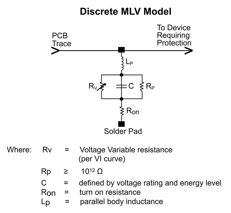
Click image to enlarge
Figure 2: An MLV equivalent model
Output matching components
A wide variety of inductors, including wire-wound ceramic, multilayer ceramic, multilayer thin-film, and multilayer organic, can be used to deliver output matching solutions in IoT modules. Higher Q factors in inductors translate to less loss in the circuit, which is especially important in low power devices, and, since tolerance can affect the spectrum purity of a system, tighter tolerance inductors can provide engineers with an effective way to increase the overall selectivity of IoT devices.
Wire-wound ceramic inductor product offerings include ultra-compact inductors that provide high Q factors with high current ranges, have tight tolerances (as tight as ±2%), and are designed for use in operating temperatures spanning -40°C to +125°C.
Multilayer ceramic inductors utilize a high-frequency chip construction to suit applications up to 10GHz. These inductors generally offer current ratings up to 1A and values between 0.3nH to 470µH.
Multilayer thin-film inductors feature a miniature footprint with rugged construction for reliable automatic assembly, and exhibit excellent high frequency performance, extreme lot-to-lot repeatability, and tight tolerance. The use of very low-loss dielectric materials, such as silicon dioxide (SiO2) and silicon oxynitride (SiON), in conjunction with highly conductive electrode metals results in low ESR and high Q, and these high frequency characteristics change at a slower rate with increasing frequency than ceramic microwave inductors.
Additionally, an emerging inductor technology, multilayer organics, utilizes low-loss, high Q materials to create low-profile inductors that can withstand high transient voltages without parametric shift.
Timing
Since IoT applications must synchronize with numerous other systems, accurate timing is of paramount importance and forms the basis for several critical applications, including: security, data consistency, motion detection, velocity estimation, and many others. Most IoT MCU/connectivity chips currently utilize small, high-precision crystal products, such as crystal units, clock oscillators, and TCXO devices to achieve accurate timing.
The selection of these devices requires an application-specific balance of exacting timing, size, weight, and shock withstanding capabilities to ensure that each individual system’s cost and accuracy needs can be met. For example, wearable devices generally require significantly smaller timing solutions than stand-alone devices and may be subject to more extreme cost pressures.
Connectors
Connecting wires to various IoT modules can also present a challenge, but insulation displacement connectors (IDCs) provide a particularly effective solution. Tested to automotive levels of shock, vibration, and temperature cycling, surface mount IDCs reliably connect individual wires ranging from 12–28 AWG directly to PCBs while robustly withstanding the extreme shock, vibration, and temperature conditions of harsh market applications.
This industry-proven contact system also enables simplicity of use, allowing users to insert wires into SMT contacts with a small tool or optional retention/termination cap, and facilitates the PCB connection of a wide range of devices without soldering. IDC contacts provide gas-tight connections to the conductor of the wire, the optional cap provides positive strain relief in even the harshest conditions, and, in case of repair, the wires can be removed and replaced up to three times.
Lots of opportunity
In sum, although myriad components suitable for use in the IoT device market are readily available, component suppliers will continue to develop and introduce innovative new power, input sensor, output matching, timing, and connector components especially designed to meet the unique performance demands of the rapidly expanding IoT market and enable the optimal execution of the efficiency, safety, and convenience benefits that these devices offer as they continue to proliferate and stake an ever greater claim in the modern electronic landscape.
References
1. Gartner. “Gartner Says 6.4 Billion Connected ‘Things’ Will Be in Use in 2016, Up 30 Percent From 2015.” November 10, 2015. http://www.gartner.com/newsroom/id/3165317.