Optimizing power by phase positioning
Proper phase positioning minimizes input filtering for multiple-output DC/DC switch-mode supplies
The technique of paralleling power converters and phase shifting their outputs is not new, and “interleaving” (as it is known) has been used in a number of applications to reduce the size of input and output capacitors. These include the 42V/14V DC-DC converters found in dual-voltage vehicle electrical systems and the voltage regulator modules (VRMs) used in computers to provide the multiple supply voltages needed by processors, memory chips and other components. Where each channel is identical, evenly distributed phase angles achieve the best ripple cancellation effect. More often however, several different converters share the same input power supply bus and in such cases a more optimal phase arrangement is required to minimize the size of the input filter.
To address this issue an optimization algorithm was proposed to optimize input current interleaving in a single-input multiple-output converter system and a study was undertaken to verify the results. The study used buck type converters because they have discontinuous input currents that can cause the input filter voltage to fluctuate significantly. However, the principle applies equally to other converter topologies, and even systems combining multiple topology types.
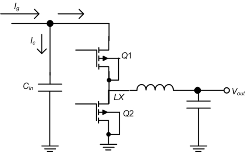
In the buck converter shown in Figure 1, the input current is discontinuous due the switching nature of the upper MOSFET Q1. When Q1 is closed at the beginning of a switching cycle, the current Iin is conducted from the input filter capacitor Cin to the switching node LX and it is equal to the inductor current; when Q1 is open for the rest of the switching cycle, the current Iin is zero. This pulsating current demand can cause a large input voltage ripple and therefore a large input filtering capacitor is usually required.
Click image to enlarge
Figure 1. A buck converter with input capacitor
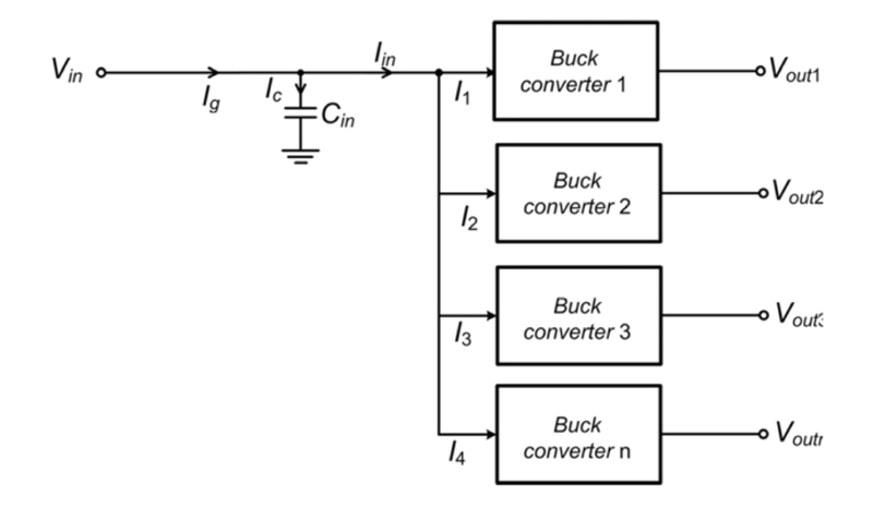
In many applications, multiple buck converters run from the same source and serve different loads on the same PCB board as shown in Figure 2. For EMI reasons, designers prefer to synchronize the switching of each converter using phase lock loops (PLLs) based on the same oscillator clock so that there is only one fundamental frequency component in the noise spectrum.
Click image to enlarge
Figure 2. Example single-input 4-channel output buck converter
Unless steps are taken to prevent it, a generic PLL implementation will synchronize all channels to switch at the same phase position, resulting in the overlap of pulsating input currents from all these channels and hence the need for large filtering capacitors. To overcome this drawback, the phase positions for the converter channels can be interleaved to reduce the requirement on the input filtering capacitance. This involves optimizing the phase angles to achieve a minimum capacitance while ensuring it is still sufficient for reliable system operation.
Solved by an optimization algorithm
The goal of the phase optimization process is to reduce the electrical and hence also the physical size of the input capacitor. The criterion used to judge the success of this technique is the extent to which the voltage ripple at the input capacitor is minimized. For the purposes of the analysis, it is assumed that once a properly sized input capacitor is applied, the pulsating input current due to the converter will be filtered such that the current from the supply to the input capacitor, Ig in figure 1, is then constant. The voltage variation on the input capacitor can then be represented by an integral of the capacitor current Ic, which is the difference between the pulsating input currents and supply current. For simplicity, it is also assumed that the input filter is composed of a single ideal capacitor without considering the effect of any parasitic components.
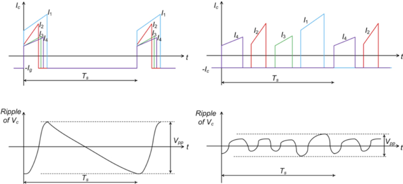
The algorithm will search for the best placements for all input currents at their nominal ratings so that the peak-to-peak voltage ripple, i.e. Vpp, is minimized. The cost function of this optimization can be described as: J = min(Vpp), referred to as the input ripple factor. The concept is illustrated in Figure 3 where phase positions of four converters, represented by their input current pulses, are shown before and after the optimizations along with the corresponding output voltage ripple. This shows that the output capacitor ripple depends strongly on the phase positioning of the converter channels.
Click image to enlarge
Figure 3. Comparing a non-interleaved system (left) with the proposed concept for phase position optimization (right)
The algorithm assumes a finite number of phase positions (p) per switching period. Hence for an n-channel system, where multiple channels can be positioned at the same position, the number of possible phase configurations can be expressed as:
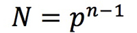
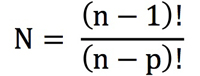
This assumes the phase position selection for the first phase is arbitrary since only the relative phase positioning between channels is relevant and therefore the first channel is always at position 0. In a system where multiple channels cannot share the same phase positions (due to controller resource sharing limitations), the number of possible phase configurations is found to be:
This allows an algorithm to be implemented as follows:
-Calculate Iavg, the average current drawn from the input supply, Ig, for the given converter parameters. This is equal to the sum of the load currents of all channels.
-Loop through all possible phase configurations. The total number of iterations is defined by either equation. For each configuration:
-Plot Iin and integrate the difference between Iavg, the dc value of Ig, and Iin, the sum of the instantaneous current drawn by all converters. This should be done for a time period corresponding to the lowest frequency of all converters and, when calculating the instantaneous current drawn by the power stages, the ripple should be taken into account.
-Determine the maximum and minimum values of the integral found above. The difference will correspond to the input ripple factor, proportional to the input voltage and current ripple.
-After iterating through all possible N phase configurations, select the one with the minimum input ripple factor.
While it might seem disadvantageous to use a numeric approach that consists of an iterative trial and error process, this algorithm is designed for implementation in the software used to configure a power supply controller, where computational resources are abundant, as opposed to being implemented in the controller’s hardware. Furthermore, the algorithm allows certain configurations to be selectively discarded, e.g. phase configurations that cause issues related to switching noise, and is therefore more flexible. A closed-form solution might be more computationally efficient, but would not allow for discarding arbitrary choices based on system limitations.