Optimizing the 800 V to 48 V/50 V Power Path for AI Data Center Servers

High-voltage conversion architectures from the 800 V bus to the processor core
Figure 1: Evolution of data center power architecture: (a) today: AC distribution, integrated IT racks; (b,c) next-gen systems: AC distribution, disaggregated IT racks with 50 V servers (b) or 800 V servers (c); (d) future systems: data center-wide HVDC, 800 V servers
The rapid growth of AI and accelerated computing is fundamentally reshaping power‑delivery requirements inside modern data centers. As GPU clusters scale towards and beyond 1 MW/rack, traditional 48 V rack‑level distribution is reaching its practical limits due to high currents, thermal stress, and increasing copper overhead. To address these challenges, hyperscale operators are now moving toward 800 V high-voltage DC (HVDC) distribution, a transition that significantly reduces distribution current and associated conduction losses while supporting the continuously increasing power density demanded by AI servers.
Within this emerging 800 V architecture, power delivery from the HVDC bus down to GPU core voltages follows a multistage conversion chain. Earlier research and recent development work have examined the full system from grid input through to the final point‑of‑load (PoL) regulators. However, for design engineers and system architects, the most critical design trade‑offs occur in the central region of this chain: the transition from 800 V to medium‑voltage (MV) rails, and subsequently to the voltage regulator (VR) stages that power the accelerators.
This article focuses exclusively on that central block; the 800 V to MV to VR conversion path and evaluates multiple architectural options using measured converter data, device‑level efficiencies, and a system‑level optimization tool developed to quantify real‑world design trade‑offs.
Why selecting the right 800 v conversion path is non‑trivial
As data center power architectures evolve toward 800 V HVDC distribution, designers face several viable pathways to step down from the HV bus to the voltages required by modern GPUs. At first glance, these options, such as converting from 800 V to 50 V, or directly to 12 V or even 6 V, may appear interchangeable. In practice, however, each pathway carries very different implications for efficiency, thermal behavior, current density, power delivery network (PDN) performance, and overall system cost.
Three architectures dominate the current discourse:
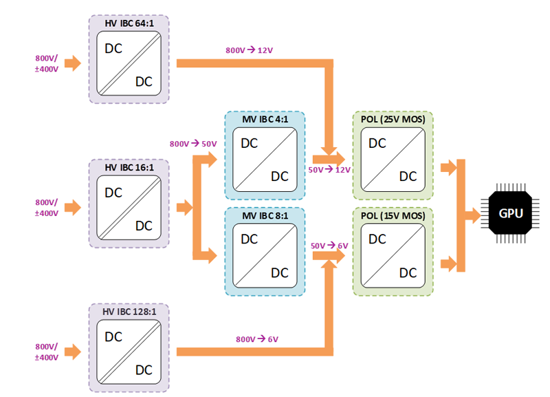
1. 800 V to 50 V to MV IBC to VR
2. 800 V to 12 V to VR (direct)
3. 800 V to 6 V to VR (future‑leaning)
Choosing between them is far from straightforward. Key constraints such as GPU power levels, allowable board areas, VR placement (top, bottom, or vertical), transient requirements, and target current density, etc. can shift the balance dramatically. Additionally, the PDN resistances between the HV IBC, MV IBC, and VR stages play an outsized role; even small variations can reorder which architecture delivers the highest system‑level efficiency.
Click image to enlarge
Figure 2: System-level design factors that influence the selection of an 800 V power-conversion path
For these reasons, selecting an optimal 800 V power‑conversion path requires a holistic evaluation rather than relying on isolated converter specifications.
Infineon’s 800 V conversion portfolio
Designing an efficient and scalable power-delivery chain for 800 V data center architectures requires coordinated optimization across three key building blocks:
· The high-voltage (HV) intermediate bus converter (IBC)
· The MV IBC
· The VR
Infineon has active solutions in all three domains, and each stage offers distinct trade-offs in performance, cost, and integration level. This section provides a high-level overview to frame the architectural choices explored later.
HV IBC: 800 V to 50 V/12 V
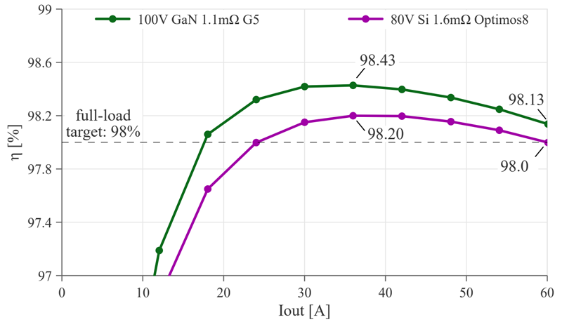
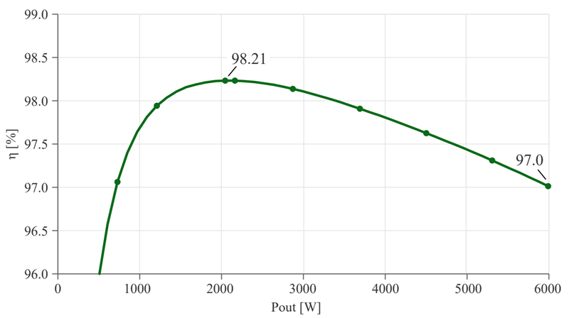
At the HV stage, two conversion strategies are commonly considered. The first is an 800 V-to-50 V high-voltage DC-X converter, which aligns with distributed 50 V architectures and achieves around 98% full-load efficiency in measured implementations.
Click image to enlarge
Figure 3: Measured efficiency curves of a single 3 kW module with Vin = 400 V and Vout = 50 V comparing Si versus GaN transistors as synchronous rectification switches
The second is a direct 800 V-to-12 V high-voltage DC-X converter, which removes an intermediate stage and reduces board-level complexity, but with slightly lower full-load efficiency of around 97%.
Click image to enlarge
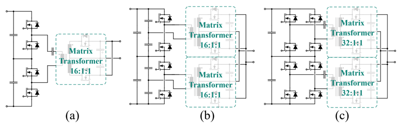
Figure 4: Evaluated topology options for the 6 kW 800 V-to-12 V DCX converter. From left to right, a) stacked Half-Bridge DCX, b) ISOP Half-Bridge DCX, c) ISOP Full-Bridge DCX
Both approaches rely on wide-bandgap devices, high switching frequencies, and advanced planar magnetics to achieve the power density demanded by next-generation AI platforms.
MV IBC: 48 V/50 V to 12 V/6 V
If the design uses an 800 V-to-50 V first stage, the next step is an MV converter to supply either 12 V- or 6 V-class inputs to the VR stage. Here, several architectural options are possible:
· a high-efficiency 8:1 intermediate-bus converter
· an 8:1 interleaved MV converter using silicon devices
· an 8:1 interleaved MV converter using GaN-enhanced switching
· a 4:1 interleaved MV converter, available in silicon or GaN-based variants
These options span different efficiency, cost, and integration points. In practice, the selected conversion ratio influences both PDN current and the operating conditions seen by the downstream VR stage.
VR stage: 12 V/6 V input
At the final step before the GPU core, multiphase VR stages translate 12 V or 6 V class inputs to <1 V rails. Designs optimized for 6 V input can use low-voltage MOSFET technology, typically delivering about 1.5 to 2% higher efficiency than VR stages built around standard 25 V MOSFET technology for 12 V input. As GPU currents continue to rise, that efficiency difference becomes increasingly important.
The system optimization tool
Selecting an 800 V power-conversion architecture cannot be done reliably by comparing the efficiency of individual converters in isolation. In a real server power-delivery chain, overall performance depends on how the HV converter, MV converter, VR, and PDN interact under load. To capture these interactions, Infineon developed a system-level optimization tool that combines measured performance data from each stage to compare complete end-to-end architectures under realistic operating conditions.
Inputs to the tool
The tool uses detailed efficiency and loss curves for each building block in the chain, derived from measured data and represented through interpolation formulas. This allows losses to be calculated accurately across the full operating range rather than at a single rated point. The model incorporates:
- Loss behavior of the 800 V-to-50 V and 800 V-to-12 V HV conversion stages
- Loss behavior of 4:1 and 8:1 MV converters
- Efficiency curves for 12 V-class and 6 V-class multiphase VR stages
- PDN resistances between the HV converter, MV converter, and VR stages, and
- The effect of VR phase scaling, where increasing the number of phases can improve efficiency under certain conditions
These inputs make it possible to evaluate a complete architecture rather than a collection of disconnected components.
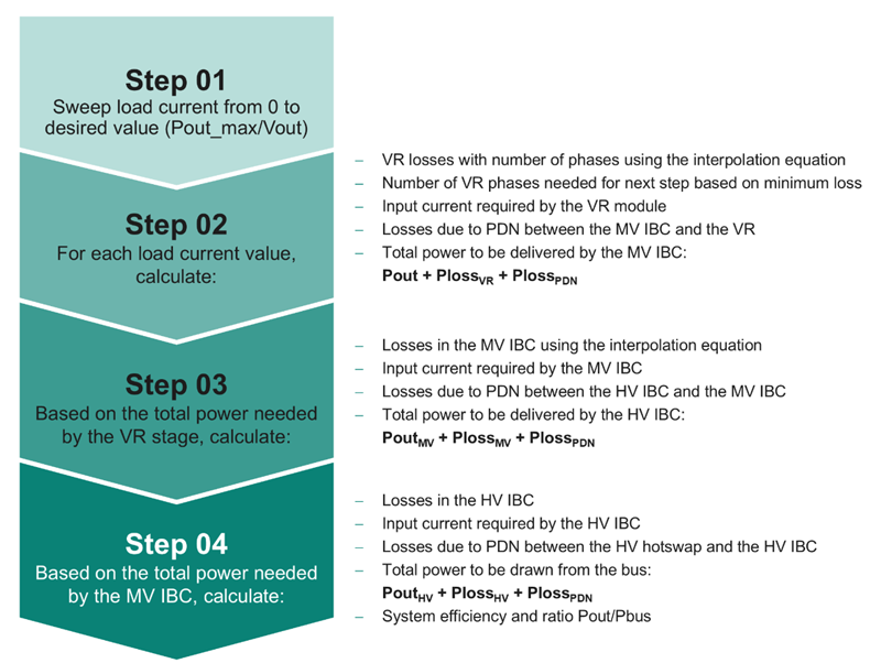
How the algorithm works
For each candidate architecture, the tool sweeps the load current from light-load to the target maximum. At every operating point, it calculates the losses in the VR stage and determines the input power required by that stage. It then adds the PDN losses between the MV stage and the VR stage and computes the power that must be delivered by the MV converter. The same process is repeated upstream for the HV converter, including the associated PDN losses.
The result is a full system-level efficiency calculation, expressed as the ratio between useful output power and total power drawn from the 800 V bus. Because the stages are cascaded, even a modest loss reduction in one block can alter the optimum architecture at system level.
Click image to enlarge
Figure 5: System-level optimization flow used to compare alternative 800 V conversion paths
Key findings from the model
The tool highlights three important trends:
1. The lowest-cost architecture is typically the direct 800 V-to-12 V path followed by a 12 V-class VR stage using standard 25 V MOSFET technology
2. The highest-efficiency architecture is often the 800 V-to-6 V path combined with a 6 V-optimized VR stage using LV MOSFET technology
3. A strong cost-efficiency compromise is achieved by an 800 V-to-50 V first stage, followed by a high-efficiency 8:1 or 4:1 medium-voltage converter, depending on PDN and VR constraints
Sensitivity to PDN resistances
One of the most important results is that PDN resistance can completely reshape the ranking of architectures. As distribution losses increase, lower-voltage VR input options can become more attractive despite requiring higher current. Conversely, where the PDN is well optimized, a cascaded 50 V architecture can remain highly competitive. In other words, the preferred topology depends not only on converter efficiency, but also on how effectively power can be routed across the board.
Vertical power delivery and the shift toward lower VR input voltages
As AI accelerators continue to increase in power and current demand, the efficiency of the final power-delivery stages becomes just as important as the efficiency of the upstream converters. This is where vertical power delivery is gaining attention. By shortening current paths between the VR and the processor, vertical implementations can significantly reduce PDN losses compared with conventional lateral layouts. That reduction is especially valuable in systems where GPU currents are already pushing thermal and routing limits.
This architectural shift also changes the preferred input voltage of the VR stage. Traditional 12 V VR systems remain practical in many designs, particularly where PDN resistance is relatively high and lower current at the board level is advantageous. However, as power modules move closer to the load and PDN resistance drops, 6 V-class VR input becomes increasingly attractive. A lower VR input voltage can improve stage efficiency, reduce heat generation around the processor, and better support the very high output currents required by next-generation AI devices.
In other words, the move toward vertical power delivery does not only affect packaging and layout; it also changes the electrical optimum of the system. Over time, this is likely to accelerate the industry transition from 12 V to 6 V VR input, with even lower input-voltage approaches potentially emerging in future highly integrated power-delivery architectures.
Example comparative scenarios
To illustrate how architecture choices play out at system level, it is useful to compare two representative approaches. The first uses an 800 V-to-50 V HV conversion stage, followed by an MV step-down stage that supplies a lower input voltage to the VR. The second uses a more direct 800 V-to-12 V conversion path, followed immediately by the VR stage.
Click image to enlarge
Figure 6: Measured converter efficiency at Vin = 800 V and Vout = 12 V over the entire load range
On paper, the direct path appears attractive because it removes one conversion stage. In practice, however, the answer depends on where losses occur.
A cascaded approach can benefit from very high efficiency in the 800 V-to-50 V stage and may reduce stress on downstream regulators by creating a more flexible intermediate distribution point. By contrast, the direct 800 V-to-12 V path can simplify layout and reduce component count, but it places greater importance on VR efficiency and PDN performance at the board level.
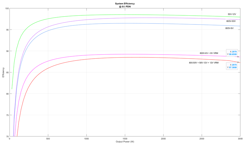
Click image to enlarge
Figure 7: Comparison of 3 stage solution (800 V-to-50 V + 50 V-to-12 V + 12 V VRM) with a 2 stage solution
(800 V-to-6 V + 6 V VRM), for ideal PDN with zero losses
When realistic PDN resistances and VR phase scaling are included, the preferred solution can shift. In some cases, a lower VR input voltage improves total efficiency by reducing losses near the processor. In others, the simpler 12 V path remains competitive because it avoids an additional conversion block. The key takeaway is that measured converter efficiency alone does not determine the winning architecture; system context does.
System protection considerations
While this article focuses on conversion efficiency and architecture selection, protection remains a critical part of any 800 V server power path. HV distribution demands robust solutions for safe connection, controlled startup, fault isolation, and system monitoring. In practice, these functions must be designed alongside the conversion stages to ensure reliability, serviceability, and safe operation in high-power AI platforms. Infineon also supports this part of the power path with dedicated protection solutions for HV systems.
As data centers transition toward 800 V HVDC distribution, the choice of power-conversion architecture between the HV bus and the processor becomes a key system-level decision. Paths based on 50 V, 12 V, or 6 V, each offer distinct advantages, but no single option is universally best. The optimal solution depends on the combined effect of converter efficiency, VR behavior, PDN losses, layout constraints, and scaling requirements.
That is why end-to-end modeling is essential. By combining HV conversion, MV conversion, VR technologies, and system-level optimization, designers can identify the architecture that best balances efficiency, complexity, and cost for a given platform. In this context, the real differentiator is not a single converter stage, but the ability to optimize the complete power-delivery chain.
References:
[1] Kasper, Matthias J.; Bernacchia, Giuseppe; Huber, Maximilian; Sanchez, Juan; Manez, Kevin Tomas; Pevere, Alessandro; Nain, Neha; Deboy, Gerald: Power Conversion Solutions for Future Server Boards Operating Directly from High-Voltage DC; https://ieeexplore.ieee.org/abstract/document/11431142
[2] Infineon Technologies: 48 V intermediate bus converter (IBC); https://www.infineon.com/applications/information-communication-technologies/hyperscale-computing/48-v-power-distribution
[3] Infineon Technologies: AI accelerator cards; https://www.infineon.com/application/ai-accelerator-card-vr-solution
[4] Infineon Technologies: Power path protection; https://www.infineon.com/application/power-path-protection


