Organic Layers Toward Efficient p-i-n Perovskite Solar Cells
Perovskite solar cells (pero-SCs) show great potential in the photoelectric fields due to high power conversion efficiency (PCE), simple processing technology, low fabrication cost, etc.. Recently, the highest certificated PCE of pero-SC has reached 25.2%, which shows great promise for the commercialization. Thus, the next research will focus on the fabrication of efficient and modular pero-SCs to further promote the commercialization of pero-SCs.
In p-i-n planar pero-SCs, the hole-transporting layers (HTLs) have an important influence on the growth of perovskite crystals, the hole transporting ability and the device stability. Therefore, developing efficient and stable HTL materials suitable for large-area processing will play a crucial role in large-area modular pero-SCs. In addition to the matched energy levels, stable chemical properties and good reproducibility, the HTL materials suitable for large-area processing should also have high hole-mobility and good wettability with the perovskite precursor solution.
Although the device based on poly(bis(4-phenyl)(2,4,6-trimethylphenyl)amine) (PTAA) as organic HTLs can achieve a PCE exceeding 22%, the poor wettability of the perovskite precursor solution will hinder the preparation of large-area modules. Up to now, new organic HTL materials in large-area devices have been rarely reported. Therefore, it is urgent to develop high-efficient and high-hole-mobility HTL materials that are compatible with large-area processing in p-i-n planar pero-SCs.
Very recently, Prof. Yaowen Li in Soochow University and co-authors designed a π-conjugated small-molecule HTL material BDT-TPA-sTh with a symmetric structure by rationally selecting the planar BDT core, TPA terminal groups, as well as conjugated 2-ethylhexyl-thienyl side chains.
The conformation and stacking model of the resultant BDT-TPA-sTh was directly observed by X-ray crystallography measurements from its single crystals. The pronounced planarity with parallel-displaced π-π and additional S-π supramolecular interactions between neighboring molecules contributed to an improved hole-mobility. In addition, the marginal solubility of BDT-TPA-sTh in the perovskite solution enabled inverse diffusion into the perovskite films, which could be used to further passivate the uncoordinated Pb2+ ion defects by Lewis-base S-atoms in BDT-TPA-sTh without damaging the under-layer HTLs.
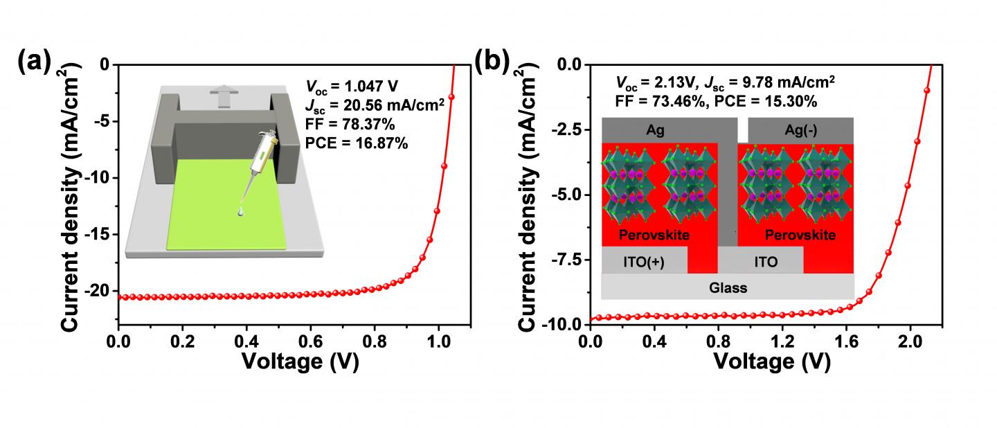
The p-i-n planar pero-SCs (Figure 1) using BDT-TPA-sTh without dopant as the HTL not only realized a high PCE (20.5%) and improved moisture stability, but also demonstrated its feasibility for fabricating large area devices through the blade-coated technology. They believe that this HTL design concept through supramolecular interactions and inverse diffusion will pave a way for designing HTL materials of perovskite-based optoelectronic devices. Their work would provide a significant progress in designing interface materials toward high performance, large area and printing p-i-n planar pero-SCs, and thus would be interesting to a wide readership for the perovskite-based opto-electronic community.
EurekAlert!, the online, global news service operated by AAAS, the science society: https://www.eurekalert.org/pub_releases/2020-05/scp-osm051220.php