Parallelized Bidirectional Switches Drive Efficiency Higher
Harnessing the high electron-mobility capabilities of GaN, bidirectional switches are revolutionizing the design of high-energy AC conversion circuits
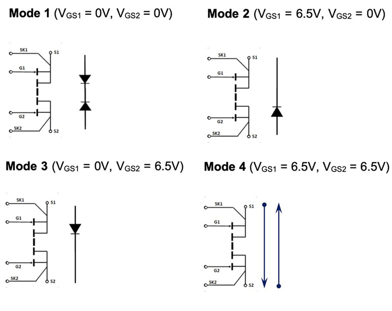
Figure 1: BDS modes
The push for efficiency in power conversion is unrelenting, especially in systems that need to deliver high power levels on a continuous basis. Though novel power-switching topologies have improved conversion efficiencies, high-power systems can benefit vastly from improvements in semiconductor technology.
Topology Considerations
Conventional topologies for high-power designs contain several power-conversion stages to convert high-current DC into grid-compatible AC. That architecture suits silicon-based semiconductor technologies, which have a preferred direction for current. This leads to the use of bridge circuits, in which different half-bridge elements engage at different points of the power cycle to either rectify an AC input or invert DC to AC. Inverters based on these topologies need DC-link elements to handle the bidirectional current of an AC output, which introduces additional resistance with resultant energy losses.
A matrix converter topology provides a potentially more efficient alternative by using bidirectional switching to eliminate DC-link elements, each of which incurs resistive losses. Though the matrix architecture has been discussed for many years, it did not find favor as conventional silicon-based power semiconductors do not support full bidirectional switching and parasitic paths allow some reverse conduction. For example, body diode of a silicon MOSFET allows reverse current flow. IGBT are required to have an anti-parallel diode to minimize reverse conduction.
In principle, it is possible to use antiparallel diodes in combination with back-to-back silicon MOSFETs or IGBTs. That comes with the penalty of higher on-resistance. Ideally, a monolithic device with single bidirectional channel is required to minimize conduction losses. Such a device has become possible following the development of technologies that implement high-mobility carriers such as GaN. The high-electron mobility of the underlying material coupled with the use of device structures to encourage the formation of a two-dimensional electron gas naturally supports current flow in either direction through the channel when it is conducting.
GaN-Based Bidirectional Switches
The bidirectional GaN switch (BDS) architecture enables engineers to leverage these high-mobility properties. Schematically, the GaN BDS can be represented as two back-to-back power switches, with the device integrating two distinct switches that share a common drain. Using the Navitas NV6428 as an example, when the gates controlling both sources are at 0V, the BDS blocks current flow in both directions and the device functions as two series-opposing diodes (see mode 1).
When the voltage on one gate increases past the turn-on threshold, the BDS becomes functionally equivalent to a diode and current can flow in one direction but not in reverse (see mode 2). In mode 3, where gate voltages are swapped, current can flow in the opposite direction. If both gates are above the threshold voltage, current can flow equally freely in either direction.
Considerations for Device Design
There are specific device-design issues that need to be considered when implementing high-performance BDS-based circuits. The substrate potential between the shared drain can change dynamically based on the different states of each source. Ideally, the substrate should be held at the lowest source voltage to prevent unwanted increases in Rds(on), which result from back-biasing or back-gating. This can be solved via substrate clamping between the two source regions and the common substrate. Doing so ties the substrate voltage to the lowest source voltage and ensures high conductivity in all modes.
A major advantage of this flexibility coupled with the low overall Rds(on) of GaN is improved performance at higher switching frequencies. To achieve similar results with silicon devices would demand the use of parallel structures that are difficult to control and balance. Furthermore, BDS GaN offers lower resistance than silicon in serial circuits and paralleling brings the ability to reduce losses even further in high-current circuits.
With parallel circuits based on unidirectional devices, paralleling demands care to ensure equal loading across the individual circuit paths. Additionally, even with GaN devices that exhibit zero reverse recovery, parasitic effects play a key role in determining how much current will pass through each of the parallel devices when turned on. Effects such as inductance can be problematic: they can restrict switching frequency.
Click image to enlarge
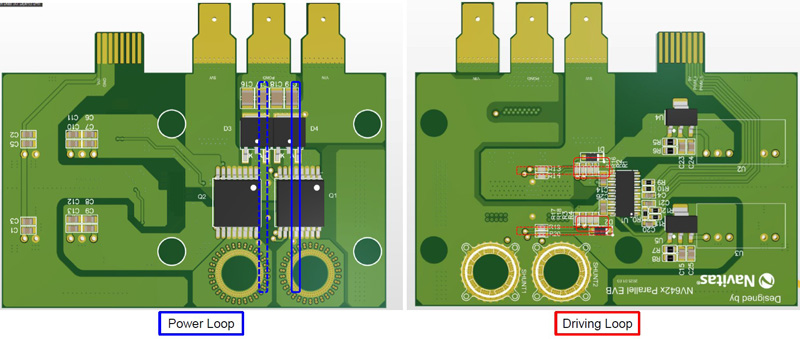
Figure 2: Example PCB layout for parallel operation highlighting the power and driving loops
Differences in inductance caused by unequal trace lengths can lead to variations in the inevitable current oscillations caused by parasitic inductance and capacitance interactions,when each device turns off. The time difference in current peaks across different devices can represent as much as 25% of the switching time. A balanced layout can reduce this effect significantly.
PCB layout is also important to BDS GaN in both serial and parallel configurations, and tests confirm these devices deliver stable, predictable performance in parallel circuits that operate at high switching frequencies. The bidirectional nature of the switches coupled with their high conductivity up to switch-off helps reduce the oscillation effects encountered with unidirectional switches in antiparallel configurations.
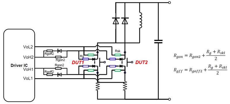
To control switching behavior precisely when using BDS devices, attention to the gate-driver configuration and layout is required. It is recommended that two floating gate driver channels are used to deliver PWM-generated gate drive inputs to the pair of gates on each BDS. One of the two gates should not be referenced to ground or a DC rail. Handling this situation requires a drive channel that can float to high voltage, and which can match the range of the source it is driving.
In some applications, both sources are switching nodes. Both the gate-drive outputs and the power supplies for them must be able to float in order to remain referenced to the source being driven. With some circuits, a ground-referenced power supply is sufficient. In other cases, an isolated floating power supply for one or both gate drives may be required.
A further recommendation is to employ isolated drivers that can turn on both gates simultaneously when bidirectional operation is needed. This approach should also be followed for parallel devices to prevent excessive loading on one of the paths. Furthermore, optimizing the PCB to reduce the length of the power and gate-drive loops will help minimize the impact of parasitic inductance, and a further consideration should be the use of resistors on both the gate-drive inputs and the source-driver connections in order to suppress gate ringing during switching.
Click image to enlarge
Figure 3: Resistor placement and calculations for the gate drivers
Performance of GaN BDS Under Test
Tests confirm that with these relatively simple design improvements, reliable operation at high switching frequencies is readily achievable.
As per the JEDEC and IEC standards, such as JEP182 and IEC60747, the double-pulse test is an important method for showing the desired behavior. This test provides the ability to evaluate rapid switching performance and losses through parasitic effects under the kinds of high-current and high-voltage conditions expected to be encountered with the loads used in real-world applications.
Using brief pulses in this type of testing will limit the impact of self-heating in the device under test and help to maintain a stable junction temperature. This in turn minimizes possible errors in evaluation that can be caused by changes in conductivity with temperature.
To perform the tests, an arbitrary waveform generator initiates two pulses in succession. The width of the first pulse is tuned to deliver a desired amount of test current through the load, with the test equipment measuring the turn-off delay, fall time, and changes in voltage and current at the end of the pulse. This initial pulse will then be quickly followed by a second pulse designed to evaluate turn-on performance and which will often reveal effects such as current overshoot. Here, the pulse should be kept short enough to ensure stable measurements without excessive heating.
As well as showing device performance, the double-pulse test is also highly effective at showing how well-balanced devices are in a parallel configuration. With devices that are difficult to balance effectively, the current flow during each pulse will show one device dominating the other. In practical applications, this would be undesirable as it implies one device will suffer increased stress, which in turn would lead to reliability issues. It would also prevent the circuit from taking full advantage of the improvements that are theoretically achievable with a parallel configuration.
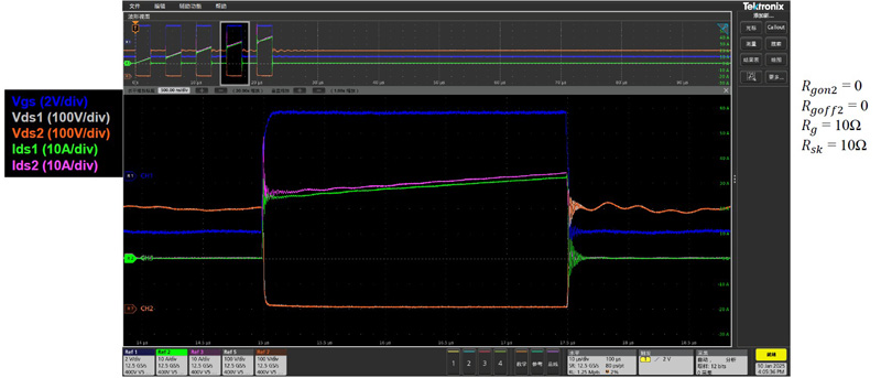
Click image to enlarge
Figure 4: Pulse test shows close match in current increase during turn-on phase
Though there will inevitably be differences in current handling between devices in a parallel circuit, small deviations are not problematic, and tests performed on the NV6428 BDS GaN devices show a difference of less than 2A when passing currents of more than 30A at peak.
Additionally, minor differences in gate threshold voltages will affect turn-on times, and this has potential implications for the low-level ringing effects seen in any switched-mode power supply, even with suppression passives in place. Ideally, these ringing artifacts will be synchronized and the double-pulse tests performed by Navitas showed this to be the case, with the current oscillations of two parallel devices during turn-off remaining entirely in phase until the current dropped to zero. Conversely, tests measuring turn-on behavior similarly showed a synchronized overshoot and in-phase ringing until the current flow settled, approximately 200ns afterwards.
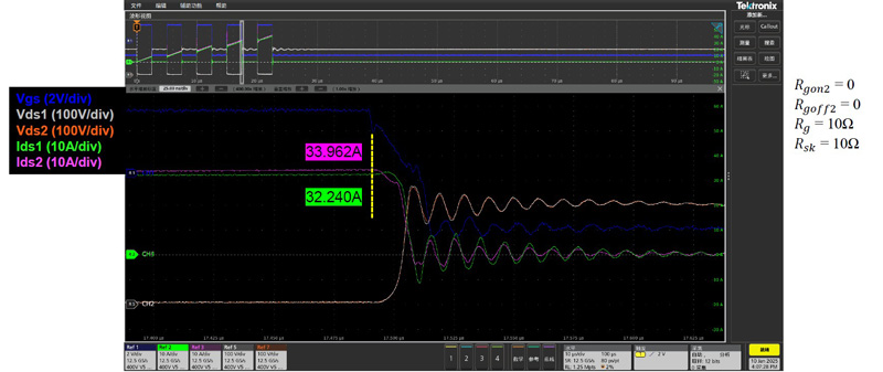
Click image to enlarge
Figure 5: Synchronized oscillation for parallel devices in both voltage and current
These tests were performed at ambient room temperature and under elevated-temperature conditions at 120°C, with results remaining consistent apart from expected changes in turn-on and turn-off losses. To help maintain good thermal performance, Navitas supplies the NV6428 and similar devices in top-cooled surface-mount packages with gull-wing leads.


.jpeg)