For switching regulator designs
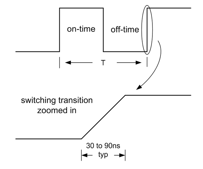
Figure 1: Switching frequency vs. switching transitions
Switch mode power supplies convert one voltage to another. Such supplies are generally very efficient and thus replace linear regulators in many applications. Switching frequency versus switching transitions Switch mode power supplies operate with a certain switching frequency. This switching frequency may be fixed as in PWM type control or it may vary depending on certain factors as in PFM or hysteretic type control. In any case, the principle which makes switch mode power supplies work is that there is a certain on-time period, Ton, and a certain off-time period, Toff. Figure 1 shows a typical switching cycle with 50% duty-cycle. This means that 50% of the length of the complete period T we have a certain current flow in the converter and during the other 50% of the time we have a different current flow. The actual switching frequency, in other words length of the period T, is not so important when we consider system noise. This switching frequency or its harmonics may hurt us if it is in the range of a delicate signal frequency in the system. But generally this frequency is not what hurts us the most. What is really critical in switch mode power supplies is the speed of the switching transitions. In the bottom part of figure 1 we can see the switching transition zoomed in the time scale. At a time scale of 2us per period T, with 500kHz PWM switching frequency, the transitions look like vertical lines as shown in the top part of figure 1. Zoomed in, as shown on the bottom part of figure 1, we can see that switching transitions are typically between 30 to 90ns.
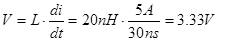
Why good printed circuit board layout is so important Every 2.5cm of board trace has about 20nH of trace inductance. The exact inductance does depend on the thickness and the width of the trace as well as its geometric layout but generally 20nH / 2.5cm is a good rule of thumb. If we look at a buck regulator for 5A of output current, we will see current switching from 0A to 5A. The following formula calculates how much voltage offset tiny trace inductance generates if the switched current is large and the switching transition time is short: With 2.5cm of trace (20nH), 5A output current (5A of switched current in a buck) and a transition time of a MOSFET power switch of 30ns we get a voltage offset of 3.33V.

This voltage offset resulting from only 2.5cm of trace inductance is quite significant. Often this offset even yields to switch mode power supplies not working at all. Putting the input capacitor a few cm away from the input pins of a switching regulator will usually prevent the power supply from working. If a power supply happens to still work with a poor board layout, it will generate excessive EMI. The only parameter we can influence in the formula above is the inductance of our traces. We can lower it by making the traces as short as possible. Thicker copper also helps reduce the inductance. The current is a parameter we cannot change since the power required by a load is fixed. The transition time is something we can but don't want to change. Slowing down the transition times will decrease the generated voltage offset and with this reduce EMI but our switching losses go up and we are forced to operate at lower switching frequencies with expensive and bulky power components.
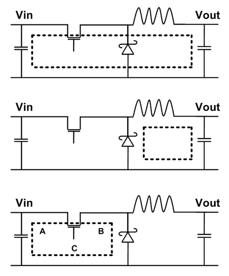
Finding AC current traces The most important rule in switch mode power supply board layout is to keep the AC traces as short as somehow possible. If this rule is followed diligently, 80% of a good board layout is already implemented. In order to find these AC traces which change current flow from �full current' to �no current' in short amounts of time, the transition time, we draw down the schematic three times. This is shown in figure 2 with a simple buck type switch mode power supply. On the top schematic, we draw a dotted line to where the current flows during the on-time. In the middle schematic we draw with a dotted line the current flow during the off-time. The bottom schematic is the interesting one. Here we display all the traces where current flow is changing from the on-time to the off-time. These traces in the bottom schematic of figure 2 are the AC traces and these have to be kept as absolutely short as possible to reduce parasitic inductances. This exercise can easily show us for any switch mode power supply topology where the AC current traces are. When evaluating existing board layouts, it is often a good idea to print them on paper, put a see through plastic sheet on top of them and use different color pens to indicate the current flow during the on-time, off-time and the resulting AC traces. Though we tend to believe that we can do this relatively simple indication process in our heads, very often we make slight mistakes in our thought process so that it is strongly recommended to do this with paper.
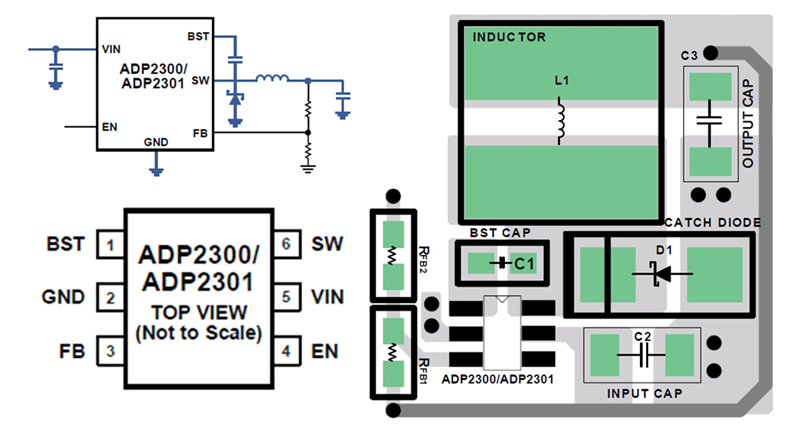
Implementing a good board layout Figure 2 shows the AC traces of a buck regulator. It is important to note that also some ground traces are AC traces and need to be kept as short as possible. Also it is recommended to not use any vias for these AC current paths. Vias also have quite high inductance. There are only very few exceptions to this rule. In cases where avoiding vias in the AC path would actually cause more trace inductance than the via itself, it is suggested to use vias. Multiple vias in parallel are better than one single via. Figure 3 shows an example board layout with Analog Device's ADP2300 step down regulator. Let's check if the AC traces are routed in the absolute shortest way possible. Figure 2 indicates AC current connections with the letters A, B and C: • Connection A in figure 5 is routed as short as somehow possible since the high side connection of C2 has the shortest trace possible to the switching MOSFET which is pin 5, Vin pin, in the ADP2300. • Connection B is the trace between pin 6, SW pin, and the cathode side of diode D1. Again in figure 5 we can see that this trace is as short as possible to reduce trace inductance. • Connection C is the trace between the anode of diode D1 and the ground connection of C2. These two component pads are right next to each other and have the lowest trace inductance possible. Also it is good for this AC current to avoid going through the silent ground plane. A ground plane should be used as reference voltage only and ideally no currents should flow through a ground plane, especially no AC currents. The vias next to C2 connect the ground area of the PCB top layer to the ground on the bottom layer, but no AC currents flow through these vias.
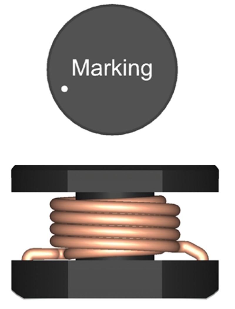
Special considerations for inductors Regarding electromagnetic interference, EMI, we also have to consider the inductor. The actual component is not as symmetrical as many people think. It has a core and wire is wrapped around it. There is always one start of winding and one end of winding connection. The start of winding is connected to the inner windings of the inductor and the end of winding connection comes from the outer windings of the inductor. Figure 4 shows the sketch of a typical drum type inductor. Often the start of winding is marked with a dot on the component. It is important to connect the start of winding to the noisy switch node and the end of winding to the silent voltage. In case of a buck regulator this is the output voltage. Then the fixed voltage on the outer windings will shield the AC switch node voltage on the inner windings electrically and the EMI of the power supply will be lower. By the way, this is also the case for so called shielded inductors. They do use some shielding material on the outside which has a certain permeability. This material will pull in most magnetic field lines on the side of the package. However, this material is only containing magnetic fields and not electric fields. AC voltages on the outside winding are mostly a problem due to electric or capacitive coupling which is not contained by the shielding material of shielded inductors. Thus also shielded inductors should be placed on the board so that the noisy switch node is attached to the start of winding for lowest EMI. Basis for a good board layout for switch mode power supplies How to do a good board layout is often not taught in engineering classes. In high frequency, RF type classes, the importance of trace impedances are studied but engineers having to build power supplies to power their systems often do not look at the supply as a high frequency system and often neglect the importance of the board layout. Most problems resulting from poor board layout can be traced back to not keeping the AC current traces as short and tight as possible. Understanding the reasons behind the presented board layout rules and following them will minimize any PCB related problems in switch mode power supplies. www.analog.com


