Power Integrations claims first Qualcomm Quick Charge 2.0 Smartphone Charger reference design
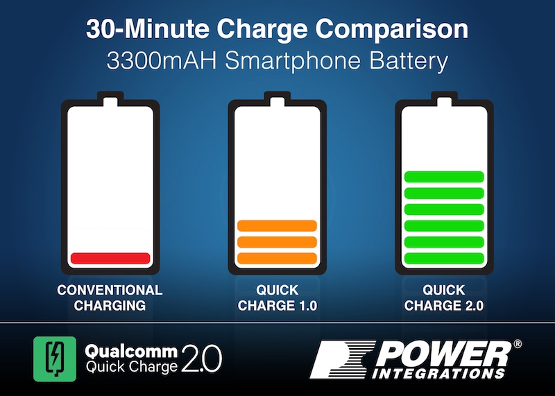
Power Integrations, a leader in high-voltage integrated circuits for energy-efficient power conversion, introduced the first reference design for a Qualcomm® Quick Charge 2.0-enabled charger power supply. Launched earlier this year, the Quick Charge 2.0 protocol from Qualcomm (Nasdaq:QCOM) enables users to charge mobile devices, such as tablets and cellphone handsets, up to 75% faster than when using conventional USB charging technology. Power Integrations has developed the ChiPhy™ family of AC-DC wall-charger interface ICs which, when combined with the company's AC-DC switcher ICs, incorporates all of the necessary elements to add rapid charging functionality to AC-DC wall chargers. The CHY100 IC detects commands from a Quick Charge 2.0-enabled device, and adjusts the output voltage of the AC-DC wall charger to deliver increased power to the device's battery through a standard USB cable. When plugged into a five-volt USB-powered device without Quick Charge 2.0 capability, CHY100 IC automatically disables the higher-voltage capability to ensure safe operation and backwards compatibility with older hardware. An evaluation platform for ChiPhy ICs, DER-381 describes a CV/CC charger power supply capable of up to 24 W utilizing TOPSwitch™-JX switcher and CHY100D interface ICs. The PSU operates from universal input and provides selectable output voltages (5 V, 9 V, and 12 V) with a maximum constant current of 2 A. The TOPSwitch-JX IC maintains virtually constant efficiency across a very wide range of output voltages and current load conditions. According to Peter Vaughan, director of application engineering at Power Integrations, "DER-381 shows, for the first time, how a Quick Charge 2.0 charger power supply can be successfully implemented using the latest generation of Power Integrations' switcher and interface ICs and simple optocoupler feedback." Power Integrations