Power Integrity Verification with an Oscilloscope
Memory errors, lower than expected data rates, or unexplainable sensitivity reduction in receiver components can be avoided by power supply qualification
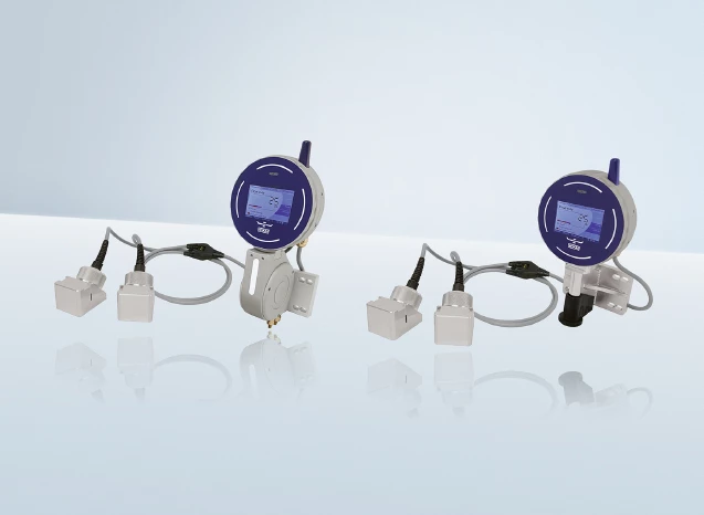
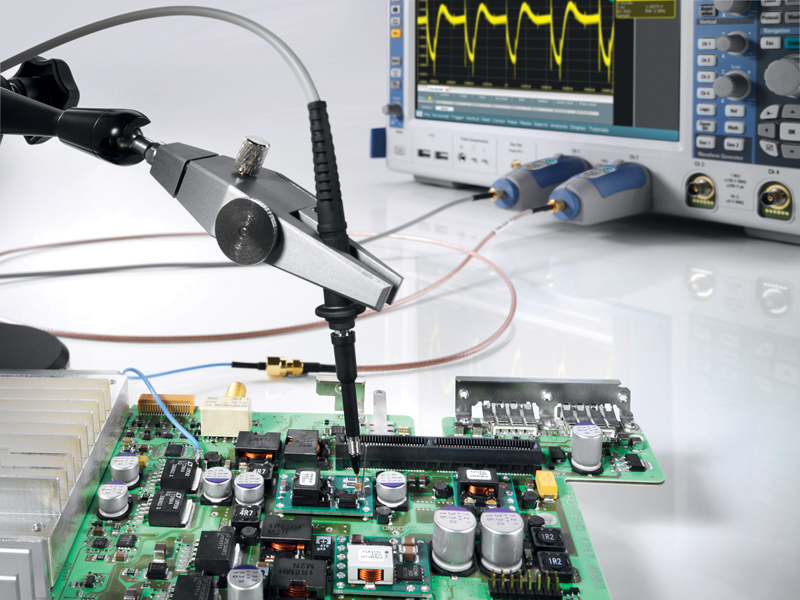
Figure 1: Two R&S RT-ZPR20 power rail probes connected to an R&S RTO oscilloscope. One is connected to a coaxial cable soldered directly into the circuit, while the second has an attached browser module for quick overview measurements. Source: Rohde & Schwarz
In the worst case, advanced electronic designs can have up to a hundred power supply networks with different DC voltages. Each power supply network has its own requirements for DC voltage accuracy and maximum allowable disturbance signals. Unwanted disturbance signals on the DC power supply network can lead to EMC problems or impair circuit operation. Power supply networks for CPUs, memory components or FPGAs are especially critical. With the required DC supply voltages steadily dropping, the allowed DC voltage tolerances are becoming tighter all the time. These tolerances must be met under all load states to ensure correct circuit operation.
DDR4 memory components are a typical example. Compared with DDR3 memory components, the maximum data transmission rate increases from 2133 Mbit/s to 3200 Mbit/s. With DDR4 memory components, the clock period is just 313 ps, and in many cases half of that is needed to accommodate clock and data jitter. Unwanted disturbance signals on the supply voltage increase clock and data jitter and can lead to data transmission errors. At the same time, with DDR4 memory components the maximum tolerable ripple on the DC supply voltage is reduced to 60 mV (Vpp) with a 1.2 V DC supply voltage. To avoid memory errors, compliance with this tolerance window is required in all operating states.
Preferred measuring instrument: an oscilloscope
The preferred measuring instrument for power integrity measurements is an oscilloscope. It lets users check the level and quality of supply voltages, and at the same time enables them to analyze disturbance signals on the power supply in the time and frequency domains and identify possible causes.
In the past, passive probes were usually used for these measurements. However, they have significant drawbacks for verification of power supply networks in advanced designs:
· High sensitivity is only possible with 1:1 probes, but their bandwidth is typically limited to less than 40 MHz. Brief voltage dips due to fast load changes or high-frequency disturbance signals cannot be visualized with these probes.
· Significantly higher bandwidth is possible with passive 10:1 standard probes, but only with distinctly lower sensitivity. Verification of the tight tolerance limits of advanced electronic components is therefore not possible.
· With passive probes, the offset range is determined by the oscilloscope and is often only max. 1 V at the most sensitive setting. This is almost always insufficient to compensate for the DC component of supply voltage networks. Although the DC component can be eliminated by using AC coupling or blocking capacitors, in that case it is not possible to reliably determine whether the measured ripple voltage is actually within the tolerance window or the supply voltage drift violates the tolerance limits.
· With measurements made using standard probes, the DC accuracy is limited by the oscilloscope. It is typically about 2 %, which is nearly as large as the allowed supply voltage tolerance for advanced FPGAs. Complete supply voltage verification is therefore not possible with standard probes.
Power rail probes offer decisive advantages
The combination of high sensitivity, wide measurement bandwidth, large offset range and high DC accuracy can only be achieved with probes specifically designed for this purpose. Rohde & Schwarz offers the R&S RT-ZPR20/40 power rail probes (Fig. 5) for this application. They combine an active circuit portion for low frequencies with a passive circuit portion for high frequencies to provide decisive advantages for the qualification of power supply networks:
· High sensitivity and low noise
Thanks to 1:1 transmission of the measurement signal, a resolution of 1 mV/div can be attained on the oscilloscope (or even 500 µV/div with the R&S RTE1000 oscilloscopes). At the same time, the probe raises the internal noise level of the oscilloscope by only 10 percent. This enables accurate, low-noise and wideband disturbance voltage measurements.
· Large measurement bandwidth up to 4 GHz
Advanced Internet of Things (IoT) designs frequently combine RF transmit and receive paths with CPU and memory components in very close proximity. An unfavorable layout or insufficient decoupling of the power supply network can lead to coupling of wideband disturbance signals into the power supply network. These disturbance signals can trigger intermittent or periodic circuit malfunctions.
With 2 GHz bandwidth, most high-frequency disturbance signals can be reliably detected with the R&S RT-ZPR20 power rail probes. The R&S RT-ZPR40 probe is specifically designed for measurements on embedded components in the mobile and IoT sectors. It offers 4 GHz bandwidth and can detect coupled-in signals in the ISM band at 2.4 GHz and the LTE band at 3 GHz, as well as higher-frequency RF bands up to 4 GHz.
· DC offset range of ±60 V
Most digital power supply networks work with voltages below 5 V. However, significantly higher offset voltages are necessary if analog power supply networks also have to be analyzed. High voltages are usually necessary in those situations, and disturbance signals on the power supply network of analog components are often very significant for measurements.
· DC accuracy of 0.1 % with integrated 16-bit voltmeter
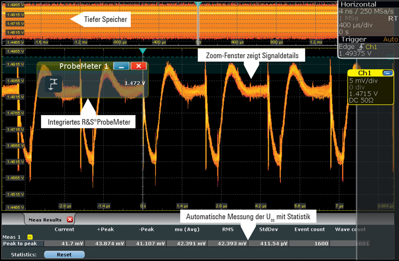
In addition to the overall signal, the power rail probes measure the DC component of the supply voltage using an integrated 16-bit voltmeter with a typical accuracy of 0.1 percent. The measured value is sent to the oscilloscope via the probe interface and shown on the display (Fig. 2). This enables exact verification of supply voltage tolerances with a single probe. It also makes the probe especially attractive for automated tests because an additional DC voltmeter is not necessary.
Click image to enlarge
Figure 2: The R&S RT-ZPR20/40 power rail probes have an integrated R&S ProbeMeter. Along with high resolution signal details such as ripple, noise and transients, they display the exact DC voltage of the power supply network on the oscilloscope. Source: Rohde & Schwarz
The right connection
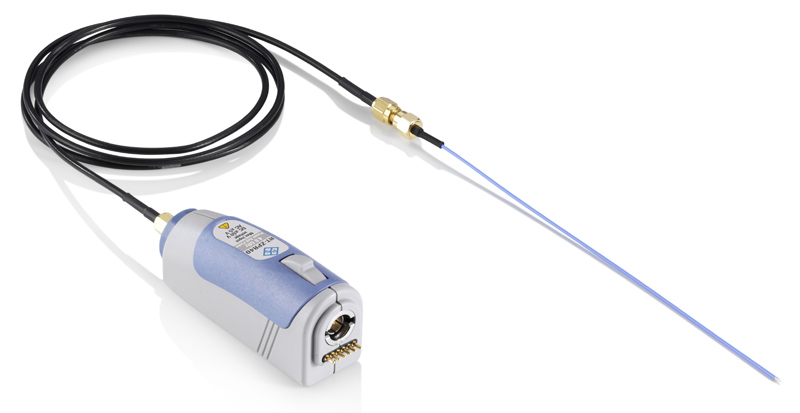
There are a number of ways to connect a power rail probe to the supply voltage on a printed circuit board. The included 350 MHz browser is particularly suitable for quickly checking several power supplies in an electronic design. This is a probe tip that attaches to the SMA connector of the Rohde & Schwarz probe adapter. Ground spring contacts to minimize ground loops and clips for connection to components or test points are also included. A good connection is required for precise, low-noise, wideband measurements. The included 50 Ω SMA coaxial cable (pigtail cable) is often used for this purpose. It can be soldered to a test point to provide a low-noise, wideband connection (Fig. 3).
Click image to enlarge
Figure 3a: R&S RT-ZPR40 power rail probe with Rohde & Schwarz probe adapter cable and attached 50 Ω SMA pigtail coaxial cable for soldering into the circuit. Source: Rohde & Schwarz
Click image to enlarge
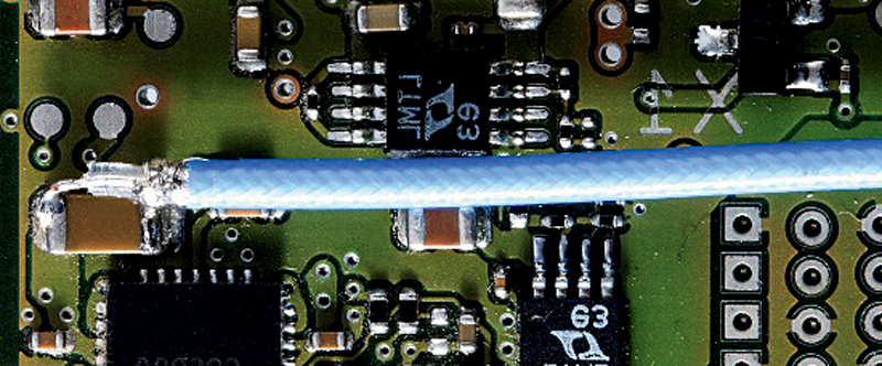
Figure 3b: Solder-in pigtail coaxial cables preserve the probe bandwidth and provide excellent connection exactly where the measurement needs to be made.Source: Rohde & Schwarz
Example: Measuring supply voltages for DDR4 memory
Measurements on supply voltages for DDR SDRAM memory need to be made as close to the memory component as possible. The solder-in pigtail cable is a good choice for this. If the memory component is driven by an FPGA, the spyhole method is recommended. An unused FPGA pin is used to measure the DDR core voltage directly from the FPGA. The DDR core voltage is applied to this I/O pin, and then the pin is probed externally with the power rail probe. This is often the closest place to the supply voltage that a measurement can be made.
The following two methods are often used to qualify a power supply network:
Peak-to-peak voltage measurement in persistence mode
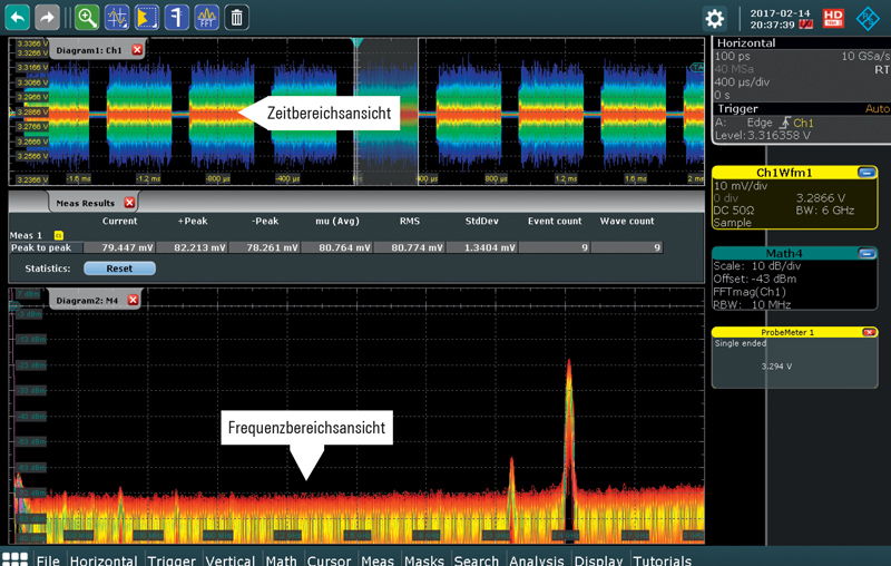
The user can employ the infinite persistence mode (infinite persistence duration) of the oscilloscope to capture and display all noise events. When combined with automatic Vpp measurement and statistics display, the maximum noise voltage can easily be determined. Oscilloscopes with a high update rate, such as the R&S RTO or the R&S RTE with an acquisition rate of 1 million waveforms per second, deliver reliable measurement results within seconds. They also performhardware-based FFT measurements and display near-realtime spectral plots. This allows users to identify disturbance signals immediately (Fig. 4).
Click image to enlarge
Figure 4: The spectrum analysis function of Rohde & Schwarz oscilloscopes is a valuable tool for identifying coupled-in disturbance signals on DC power supply networks. In this example, a coupled-in 2.4 GHz WLAN signal is clearly visible. Source: Rohde & Schwarz
Triggered measurement of load step response
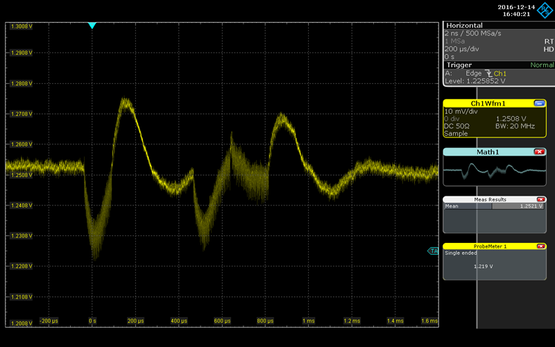
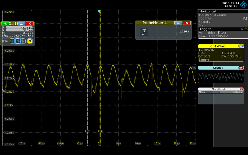
The response of a power supply network to load step changes is also of particular interest. For this measurement, the user configures the oscilloscope in single-trigger or normal trigger mode and then triggers on a known event. In the case of supply voltages for DDR memory, these are typically measurements of the load characteristics during the DDR initialization phase or in stress tests. The two screenshots in Figs. 5a and 5b show the measured ripple of a 1.2 V DDR4 supply voltage and the load step response of this supply voltage during the initialization phase of this memory component.
Click image to enlarge
Figure 5a: Measuring the load step response of a DDR4 supply voltage during the initialization phase of the DDR memory. Source: Rohde & Schwarz
Click image to enlarge
Figure 5b: Measuring the ripple on a 1.2 V DDR4 supply voltage and exact determination of the DC level with the R&S ProbeMeter – a precision DC voltmeter integrated into the probe.Source: Rohde & Schwarz
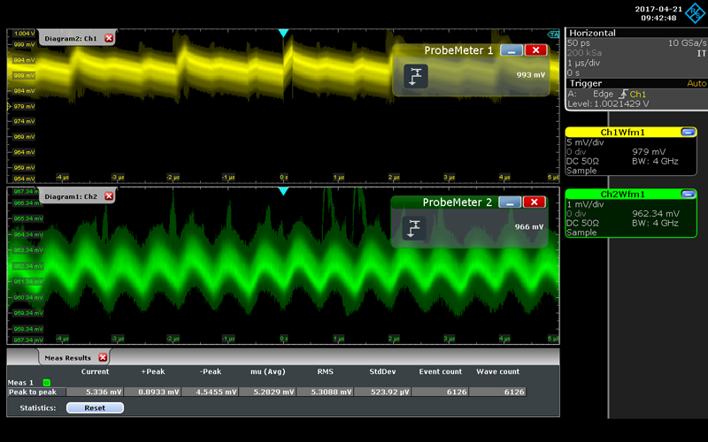
FPGA- or ASIC-based signal processing solutions often pose major challenges to power supply networks. Changing activity phases can lead to very large and fast load step changes. Figs. 6a and 6b show the load step response of an FPGA power supply to a load step change from 30 A to 60 A. The signal at the output of the DC/DC converter is shown in yellow, and the signal at the power supply pin of the FPGA is shown in green. At the same time, the integrated DC voltmeters of the power rail probes are used to display the exact DC supply voltage at the test point. The voltage drop on the PCB after the load step change to 60 A is clearly visible.

Click image to enlarge
Figure 6a: Step load response of an FPGA power supply to a load step change from 30 A to 60 A. Source: Rohde & Schwarz
Click image to enlarge
Figure 6b: Ripple on an FPGA supply voltage with 60 A load. Source: Rohde & Schwarz
Rhode & Schwarz