BUS signal integrity and noise rejection utilities
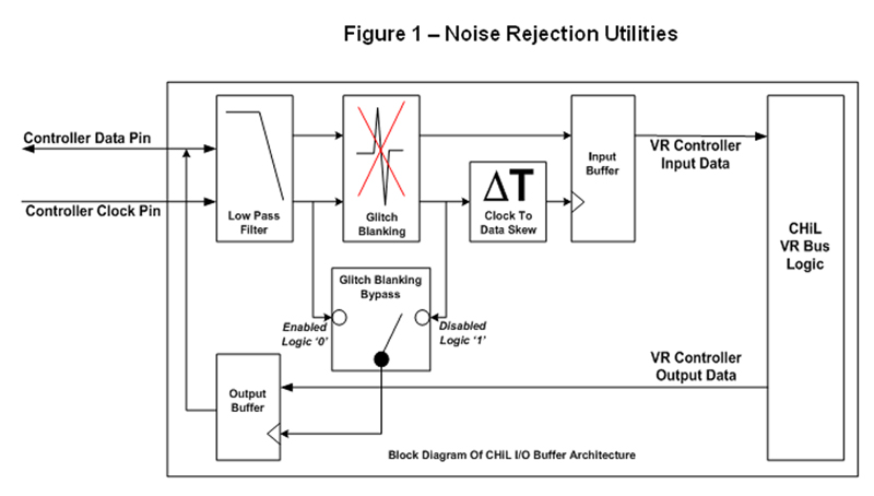
Figure 1: Noise Rejection Utilities
Modern power systems feature high speed serial communication between load and voltage regulators (VR) to enable sophisticated power management operations. This communication is susceptible to environmental noise coupling that can corrupt digital transmission. In the worst case, noise corruption can break synchronization between clock and data, resulting in regular data transmission errors. Some failure modes are periodic and can lead to repetitive communication errors that lock-up the bus even after the channel is reset. This can have a negative effect on the functionality or performance of the system powered by the voltage regulator. In computer systems, communication failures can result in �blue-screening' or system lock up. The bottom line is that noise is always present, whether from phase node coupling, cross-talk from neighboring transmission lines, ringing, or superposition of noise sources. The challenge is to guarantee good noise immunity that avoids data transmission errors. Application of transmission line theory and good layout practices are the standard methods of minimizing noise generation. However, noise is not predictable, so failure to detect a noise generator may force a board spin when analog VR controllers are used. Analog circuits require a quiet layout to avoid noise corruption. They do not have the intelligence to distinguish noise from the digital signal they are trying to receive. By contrast, digital filtering uses intelligence to distinguish data from noise, thereby providing superior noise immunity in noisy power management bus designs. Designers can optimize powerful digital filter parameters in noisy environments to restore reliable data communication, thereby removing schedule risk and cost of undesirable board spins. How is this done? One way is through the use of noise rejection utilities that repair high speed data communication failures. An example is controllers made by CHiL, which feature a digital control engine configured by a user-defined program stored in VR memory. Prior to power on, the noise rejection utilities can be programmed to aggressively filter noise. Programming is accomplished using CHiL's Intuitive Power Designer software, a companion to CHiL's VR controller chip. During validation, the filter settings can be further configured to achieve the optimal system response. What causes noise corruption? An incorrect exchange of data between master and slave is defined as a communication failure. Communication failures may occur when noise superimposed with the power management waveforms results in an invalid crossing of the receiving agent's input logic threshold voltage; this is known as noise corruption. Noise corruption is separated into two categories, data signal corruption and clock signal corruption. Data signal corruption may occur if noise violates the input threshold voltage at the receiving agent's data pin during the setup/hold window. In these cases, the error can be flagged by the parity bit and a resend of the data has the potential to correct bad communication. Clock signal corruption can lead to the most severe communication failure - loss of synchronization between clock and data, resulting in repetitive transaction errors. This occurs when a noise glitch crosses the clock's input voltage threshold and is detected by the receiving device as a valid signal. When this occurs, the data associated with the clock signal is latched into the receiving device twice - once by the noise glitch and once by the true clock signal. As a result, the data input of the receiving device is no longer synchronized with the clock; all future reads and replies are off synch by the number of detected noise glitches. The corrupted data pattern is read as an incorrect reply by the bus master or as an incorrect instruction by the bus slave. Eventually, the bus master will detect incorrect replies and attempt to reset the bus. However, as noted above, it is likely that a noisy environment will repetitively disrupt communication causing regular performance degradation of load operations. What are the noise rejection utilities? CHiL adopts three utilities for noise immunity: low pass filters, glitch blanking utilities, and a variable clock to data line skew. Each utility features user programmable settings that require no external components. The utilities are configurable on the fly using CHiL Intuitive Power Designer software, and take less than five minutes to optimize. This eliminates hours of debug that might otherwise be required, thereby reducing the risk of board spins, and ultimately speeding time to market. Figure 1 shows a general block diagram of the noise rejection utilities.
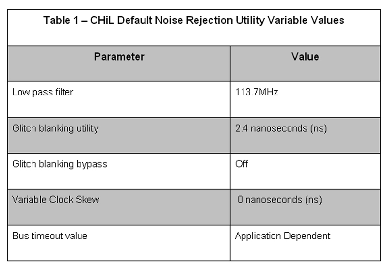
The low pass filter is in series with the signal trace and the buffer input for both clock and data nets. This feature allows the VR designer to filter out high frequency noise associated with pulse ringing, crosstalk, and phase node coupling. The variable cut-off frequency reduces intermittent coupling from neighboring fields. It offers significant attenuation of coupled phase noise with a standard 20dB per decade roll-off. The glitch blanking circuitry is also in series with the signal line and the buffer input for both clock and data nets. The receiver ignores pulse widths shorter than a programmable value. This circuit is configurable to �blank' or ignore noise-related glitches that appear as artificial data or clock pulses. The receiver rejects threshold violations from crosstalk, pulse reflections, and coupled phase node noise. To minimize the impact to the controller's time from clock to output (Tco) specification, the clock signal path can be configured to bypass the glitch blanking circuitry. The variable clock skew variable introduces a programmable skew (delay) between the clock and data at the VR receiver input, providing additional hold time at the cost of setup time. This is effective for shifting the setup/hold time window away from periodic noise. When noise corruption disrupts data transfer, the bus master will traditionally reset communication by stopping the clock. The bus timeout value variable allows the VR designer to program the timeout duration based on specific application requirements. The bus master is a CPU, GPU, or validation tool that controls the bus operation and transmits the clock. Digital noise rejection utilities ensure robust and error free communication in noisy environments Adoption of digital utilities enables the industry's strongest noise tolerance, providing superior noise margin across all manufacturing variables. Runt pulses due to transmission line reflections are ignored using the glitch blanking utility. Noise coupled from the phase node is attenuated by the low pass filter and rejected by the glitch blanking utility. Ringing from trace inductances is attenuated using the low pass filter and rejected by the glitch blanking circuit. Runt pulses resulting from cross-talk are ignored using the glitch blanking utility. In addition, the setup/hold time window can be shifted to avoid periodic noise using the variable line skew. The most impressive feature of the digital noise rejection utilities is an immediate reaction. Enabling the utilities results in immediate noise rejection, versus a 2-month design cycle spent correcting issues with a board spin. Greater noise immunity and reduction of the chance of intermittent issues gives designers higher confidence of a reliable design. Noise injection experiments demonstrate effective repair of the communication channel To verify reliability and robustness of the noise rejection utilities, CHiL conducted experiments in which noise was injected onto a high speed bus clock. The communication integrity was then observed with utilities turned off and compared to those enabled with optimal settings. The experiment used two separate boards; one for the device under test (DUT) and one for the bus master. High speed signals between the bus master and DUT were connected using long fly-wires. The clock fly wire was wrapped in multiple loops and placed close to an inductor to enable noise pick-up. A 10-amp load was then drawn through a target phase (40 board at 10-amp/phase) resulting in fields that coupled periodic phase noise onto the clock signal. In this configuration, CHiL researchers verified noise corruption on the communication channel. Coupled noise exceeding 0.5V regularly crossed receiver input threshold levels. With the utilities turned off, the VR controller intermittently �rejected' or �not acknowledged' communication - which verified communication errors. The experiment was then repeated under a variety of conditions with the noise rejection utilities turned on and properly tuned. The VR controller reliably �acknowledged' each transmission packets without error. Data communication was found to be 100 percent% reliable in this noise polluted environment with utilities enabled and tuned.
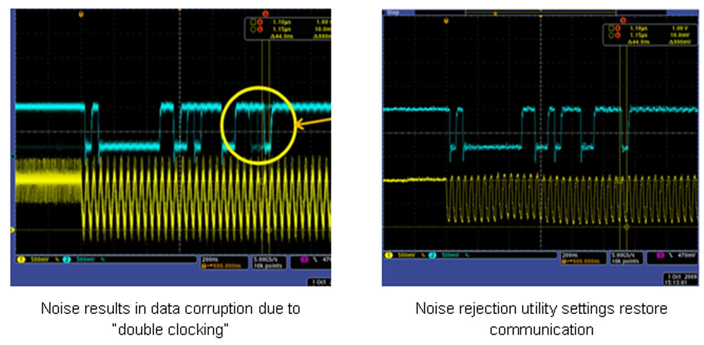
Figure 2 illustrates the results of the noise injection experiments. On the left, noise resulted in regular data corruption due to "double clocking." Repetitive commands are sent across the high speed bus with the scope triggered on the clock waveform. The circled waveform (in infinite persistence mode) shows intermittent "acknowledge" replies, mixed with "not acknowledge" and signal "reject" responses. The blue trace is the data waveform and yellow trace is the clock signal. On the right, the low pass filter is set to 114MHz and the glitch blanking pulse width is set to 2.4ns. Intermittent �not acknowledge' and �reject' replies are no longer encountered and communications is fully restored without detection of any error. The bottom line for designers is that application of transmission line theory and good layout practices are not always sufficient to avoid noise failures. Addition of CHiL's digital filtering is a designer's best option for ensuring reliable communication in noisy power designs. The outcome is reduced debug time and much faster time to market. www.chilsemi.com


