How they stack-up against the performance demands placed upon them?
Power MOSFETs have become the preferred choice as the main switching device within power supplies for a wide range of consumer and industrial electronics equipment. Because it has become more important to improve overall power supply efficiency to meet energy saving requirements from governmental and industry standards organizations as well as end users themselves, the reduction in power losses whilst allowing large load currents achieved by power MOSFETs has grown in value.
Switching speed, device temperature, power density avalanche capacity and the credentials of the device package itself are the main areas that come under scrutiny from equipment designers and where performance demands are high. Here we’ll look at the rise of the power MOSFET and how they stack-up against the performance demands placed upon them. The article then compares and contrasts established DPAK packaged devices with the newer ATPAK format from ON Semiconductor.
It is no surprise to learn that consumer demand is driving all electronic products to be smaller, lighter and lower cost while having ever-increasing functionality and feature sets. While this is true in general, the greatest focus is on modern portable devices where competition is fierce and the technology is evolving rapidly. This brings challenges in all aspects of electronic and packaging design as these requirements are often competing. As a result, engineers are called upon to make trade-offs to optimize their designs for the market.
Almost every electronic device or system anywhere has some form of power supply to convert the raw power (mains, solar or battery) to useful levels to power the device. While the power supply is essential it is often perceived to add no useful functionality. The PSU does not add any features to the device yet it accounts for a large portion of the size and weight of modern portable devices.
On top of the consumer-driven challenges, designers of modern power systems face a number of environmentally-focused challenges. Industry standards, best practice and legislation all mandate higher levels of efficiency – especially at low power and in standby mode. Ever-decreasing voltage rails mean higher currents have to be delivered with lower losses, thus compounding the challenge.
At the heart of almost every modern switching PSU is the power MOSFET. These devices are widely used in switching regulators such as AC-DC or DC-DC converters and motor controllers. They offer excellent performance in high speed switching, high breakdown voltage, high current and low power loss. MOSFETs excel in the high speed, high frequency operation required by modern switching power supplies.
In order to address these challenges, there are many types of MOSFET available on the market today – many optimized for specific applications. In selecting the ideal device for a specific power application, the designer needs to consider key parameters that will influence the ability of the end design to meet its specification.
Electrical performance is key for MOSFET selection and one of the most important criteria is the on-resistance (RDSON) as this will directly impact the efficiency and thermal characteristics of the PSU. Switching speed needs to be matched to the application although, in general, RDSON increases with switching speed so this decision becomes a trade-off for the designer.
The MOSFET needs to be correctly sized for the application. Operating temperature and breakdown voltage (BVDSS) need to be in line with the needs of the application. Package size and style need to be selected so that the MOSFET is small enough to fit the available space, yet large enough so safely dissipate the heat generated during operation.
The package itself is an important consideration in all designs. Nowadays, surface mount is the most prevalent package type, although leaded devices are still used in some power supply applications. Apart from the ability to fit in the available space the package has a critical role in transferring the heat generated in the semiconductor die to the outside world. The more efficiently this heat is moved, the greater the power density that can be achieved.
One of the most common packages used for power MOSFETs is the DPAK which has become a de-facto industry standard since its introduction. Relatively modern, the DPAK is a surface mount device with three pins and a large mounting tab for physical strength and thermal conduction. The DPAK has proved very popular due to its small size and the convenience of tape-and-reel packaging for automated manufacture.
However, there are a couple of drawbacks to the DPAK package. Firstly, the height of approx. 2.3mm is relatively good but starts to present challenges in today’s ultra-thin designs. Secondly, the semiconductor die is connected thermally and electrically to the lead frame by thin gold, copper or aluminum wires (‘wire bonding’). These wire bonds are very thin (~70um) and, even when multiple bonds are used in parallel, they limit the thermal performance and current capability of the DPAK. The thin bonds also limit the ability to reduce RDSON to the low levels needed for success in modern PSU designs.
To address these limitations, On Semiconductor has recently introduced the ATPAK (‘Advanced Thin PAcKage’) as a next-generation package for modern power designs. In terms of size, the ATPAK fits in the exact same footprint as the DPAK making it an ideal retrofit into most existing designs. However, the ATPAK height is just 1.5mm, offering a substantial 35% improvement in height which provides a critical benefit for modern ultra-thin designs (see Figure 1).
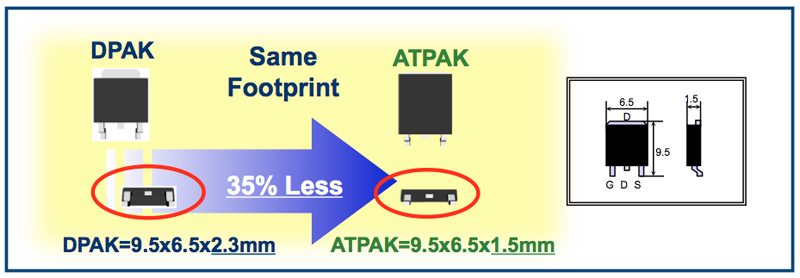
Click image to enlarge
Figure 1: The cutting-edge ATPAK has a identical footprint to DPAK yet occupies 35% less volume.
The second key innovation in the ATPAK is a new clip bonding technique that replaces the bonding wires with copper clips and brings several substantial benefits (see Figure 2). In this innovative design the copper clip connects the die to the leadframe. The copper is an excellent thermal conductor and allows better heat transfer to the pins, reducing the thermal resistance (RTHJ-A) of the package and facilitating greater power density PSU designs.
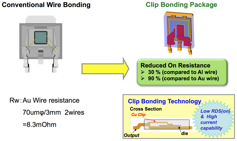
Click image to enlarge
Figure 2: The new copper clip offers much lower thermal and electrical resistance than the wire bonds it replaces.
The greater cross-sectional area of the copper clips also minimizes RDSON thus contributing significantly to reducing the losses in the PSU, thereby reducing heat generation and increasing efficiency. Additionally, the cross-sectional area increases the current carrying capability to 100A – a figure previously only achieved by the D2PAK, which has 7.5x the volume of the new ATPAK.
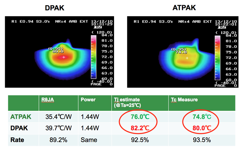
To prove the benefits of the new technology, On Semiconductor conducted a benchmark test to compare the thermal performance of the new ATPAK against the DPAK that it replaces. In this test an ATPAK device and a DPAK device were placed on identical PCBs and were both controlled so that 1.44W was dissipated in each package.
The surface temperatures were measured non-intrusively with a thermograph. The case temperature of the DPAK rose to 80°C, whereas the case of the ATPAK reached 74.8°C. By using the thermal resistance of each package the junction temperatures were calculated as 76.0° and 82.2°C for the ATPAK and DPAK respectively (see Figure 3).
Click image to enlarge
Figure 3: Thermal benchmark testing clearly demonstrated the benefits of the ATPAK deaign.
This difference of 6.2°C clearly shows the improved thermal performance of the ATPAK using the new clip bonding technique. It also shows that even though the ATPAK has 35% less volume than a DPAK it is able to dissipate heat better, leading to a lower junction temperature and greater reliability.
Clearly the cutting-edge ATPAK offers a number of real and substantial benefits that will help designers reach the challenging goals of today’s ultra-efficient, ultra-dense PSUs. The backwards compatibility makes it easy for designers to retrofit existing designs with these new devices bringing immediate benefits. With a price point very close to the DPAK, the ATPAK is a excellent choice of MOSFET packaging for all new designs.