Author:
Dr. Ray Ridley, President, Ridley Engineering
Date
06/01/2010
 PDF
PDF
This article continues the series in which Dr. Ridley documents the processes involved in getting a power supply from the initial design to the full-power prototype. In part IV, the transformer and inductor are plugged into the circuit and testing continues.
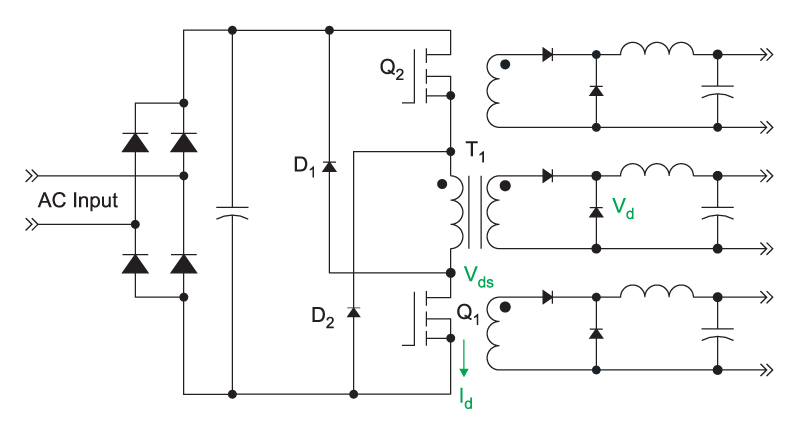
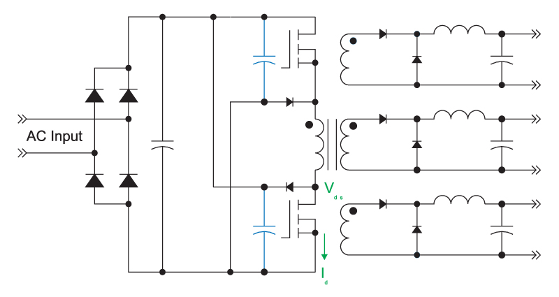
The schematic of the two-switch power stage is shown in Figure 1. Snubbers and other components are omitted for clarity.
Clcik image to enlarge
Figure 1: Power stage schematic. Some components are omitted for clarity.
In the last article of this series [1], the power stage was tested with a resistive load in place of the transformer. This allowed several issues to be resolved in the design, and verified the proper operation of the gate drives and FETs, and proper connection of instrumentation. The circuit was powered from the AC line as described in [2].
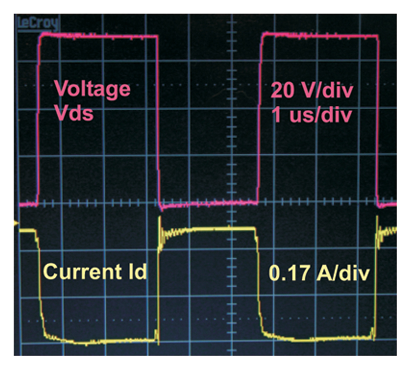
Figure 2 shows the resistive waveforms obtained for the voltage and current of the lower power FET, Q1.
Click image to enlarge
Figure 2: Lower FET voltage and current waveforms with resistive loading
Once the resistive operation was verified, the power magnetics were ready to be plugged into the circuit. The full details of the magnetics design are beyond the scope of this article, but details of changes will be described in a future part of this series. All of the magnetics were designed with the assistance of the power supply design program POWER 4-5-6 [3].
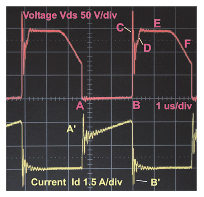
Figure 3 shows the waveforms obtained for the lower FET with the magnetics in place, and 40 VAC applied to the circuit. The red waveform is the drain voltage, and the yellow waveform is the drain current. The FET turns on at time A, and the drain voltage falls rapidly to a low value. At the same time, there is a ringing observed in the drain current, denoted by A’. This ringing is caused by the leakage inductance resonating with the capacitances of the transformer and output rectifiers.
At time B, the FETs turn off, and there is a rapid rise in the drain voltage. This is caused by the energy stored in the leakage inductance, which rings with the output capacitance of the FET, and other stray capacitances of the circuit. This voltage should theoretically be clamped to the input voltage of the power supply through the diode D1, but trace inductance causes an overshoot. This can be fixed with improved layout, as will be shown later in this article. The turn-off ringing can also be observed in the drain current at B’.
After a short period of time, the energy in the primary of the transformer is transferred to the secondary, with the exception of the energy stored in the magnetizing inductance. The magnetizing current leads to the slower rise time during the period denoted by D, after which the voltage is clamped to the input voltage through diode D1 during the period E. Once all the energy is discharged from the magnetizing inductance, the voltage falls during the period F of the cycle.
Click image to enlarge
Figure 3: Lower FET Q1 voltage and current waveforms with transformer loading at 40 VAC input
For newcomers to the field of power supply design, the initial waveforms are a surprise. The severity of the ringing at the switching transitions often makes you wonder if such a circuit can ever be made to work reliably. The waveforms of Figure 3 are quite typical of power supplies, and a considerable amount of time must be spent in reducing the effects of the ringing waveforms in order to avoid excessive noise and stress on the semiconductors.
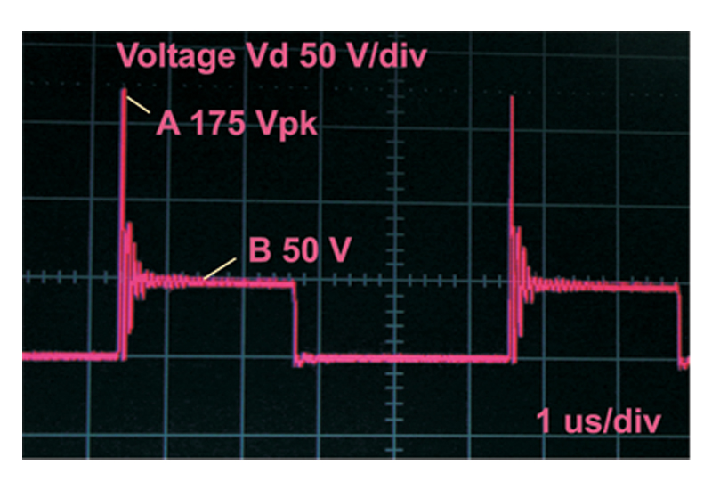
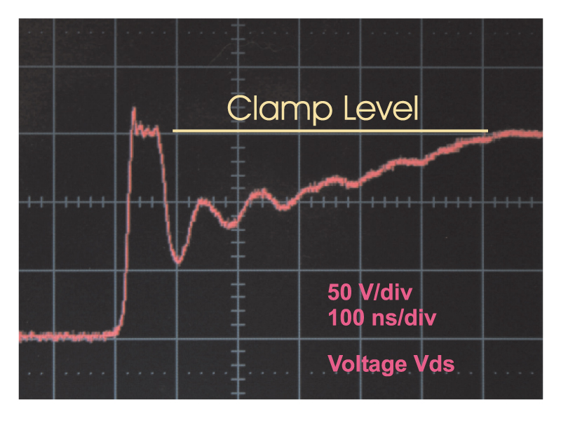
Ringing can also be seen on the secondary of the converter, as shown in Figure 4. Unlike the primary waveform on the FET, this voltage is not clamped. The peak voltage of 175 V at time A far exceeds the anticipated square wave voltage, 50 V during the main part of the switch on-time. If this is not controlled better, the secondary rectifiers will fail when full voltage is applied to the power supply. The method of controlling this spike will be the topic of the next article in this series.
Click image to enlarge
Figure 4: Secondary voltage waveform with 40 VAC applied
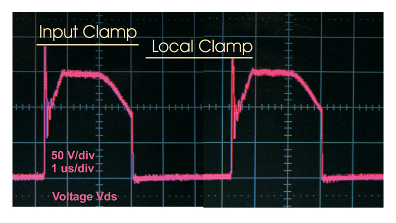
The first step in cleaning up the operation of the converter is to improve the primary clamp. The input bus capacitor was located a significant distance away from the FETs, and this introduced stray inductance in series with the clamp diodes. Mechanical board layout constraints make it difficult to place the capacitor closer. A practical solution is to add two new capacitors, as shown in Figure 5.
Click image to enlarge
Figure 5: Local capacitors added for improved voltage clamping
These two capacitors are located close to the FETs, and a very tight loop is provided from each FET through its clamp diode and capacitor. The traces from these capacitors back to the input bulk capacitor can be longer and are not critical high-frequency paths.
Click image to enlarge
Figure 6: Voltage waveforms with and without local capacitors
Figures 6 and 7 show the effects of the additional local clamp capacitors. The first waveform of Figure 6 is without the capacitors, and the second waveform includes the local capacitors. A significant reduction in the spike is achieved, and the details of this part of the waveform are shown in Figure 7.
Click image to enlarge
Figure 7: Detail of voltage waveforms with and without local capacitors
Notice how narrow the highest part of the spike is, less than 10 ns. Controlling ringing frequencies like these is difficult, but they can be very destructive despite the short duration.
When the power stage was first turned on with the main transformer in place, the gate drive immediately shut down. This was due to the current sense resistor not being replaced when the current transformer polarity error was fixed as described in the last article. (The current-sense transformer was a socketed part since it was anticipated to be changed several times to fine-tune the circuit protection.)
With the current sense resistor in place, excessively high currents were immediately seen on the primary of the converter. A small bridge of solder was discovered on the secondary side of the power transformer. This is a common occurrence when building prototype boards, even on a PCB. It also happens on production supplies â€" many times in reviewing designs as a consultant, I find that power parts have insufficient spacing for the high voltages that will be encountered, and the large parts that will be mounted on the board.
The introduction of magnetics into the power supply gives rise to significant high frequency ringing waveforms on all of the semiconductors. It is important to control the ringing spikes. One approach to this is to minimize trace inductance on the board. This is demonstrated in this article for the improved primary voltage spike with additional local capacitors.
In the next article of this series, the secondary ringing will be properly controlled with the addition of snubbers and clamp circuits.
1.“Power Supply Development Diary Part III�, Ray Ridley, Power Systems Design Magazine, May 2010.
2.“Testing Offline Power Supplies�, Ray Ridley, Power Systems Design Magazine, January/February 2010.