This article continues the series in which Dr. Ridley documents the processes involved in taking a power supply from the initial design to the full-power prototype. Initial testing on a new five-output design shows the cross-regulation achieved.
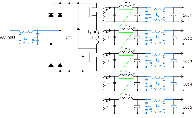
Five-Output Coupled-Inductor Design
With the second turn of the printed circuit board, the specifications were modified as follows:
1. Output 1 â�" 32.5 VDC @ 7A isolated
2. Output 2 â�" 32.5 VDC @ 7 A isolated
3. Output 3 â�" 32.5 VDC @ 7A isolated
4. Output 4 â�" 32.5 VDC @ 7 A isolated
5. Output 12 â�" 12 VDC Bias power and regulated output, primary referenced
6. Maximum power 350 W (only one output fully loaded at a time, application is for audio.)
7. Input â�" 180 â�" 265 VAC
8. Power Topology: Two-switch forward
Notice that the voltage levels are adjusted somewhat from the original design with three outputs. As a power supply designer, it is always a good idea to be flexible to system changes that come from the power supply users. This almost always happens during a product development cycle.
Figure 1 shows the schematic of the five-output forward converter. A single core inductor, L1, is used with five windings, one for each of the outputs. This coupled-inductor approach provides the best cross-regulation between each of the outputs. There are two major advantages of coupled inductors â�" firstly, all of the outputs are tied together through the transformer action of the inductor, preventing them from having individual resonant frequencies. Secondly, regardless of individual loading on each of the outputs, the coupled inductor forces all of the outputs to be in either continuous or discontinuous mode concurrently, greatly improving the regulation.
As shown in an earlier part of this series, excellent regulation was achieved with a wide variation of output loading for three outputs. With the new design, it is important to establish the cross-regulation with the two extra outputs.
Click image to enlarge
Figure 1: Forward Converter with Five Coupled-Inductor Outputs
Notice that Figure 1 shows common-mode filters on all of the power outputs. These filters are essential for proper testing of the converter, as discussed later.
Short-Circuit Testing
The new revision of the power supply design had substantial changes, including new specifications, transformer, inductor, layout, gate-drive transformer and current transformer. Before testing for steady-state operation and cross-regulation, it is very important to make sure that the new power stage design remains rugged under all conditions.
Most designers are often reluctant to subject their new board to stress testing, but it is very important that this be done in order to confirm the viability of a new design. High-line, short-circuit testing verifies that the current-limiting circuit is working properly, and that the circuit is well protected.
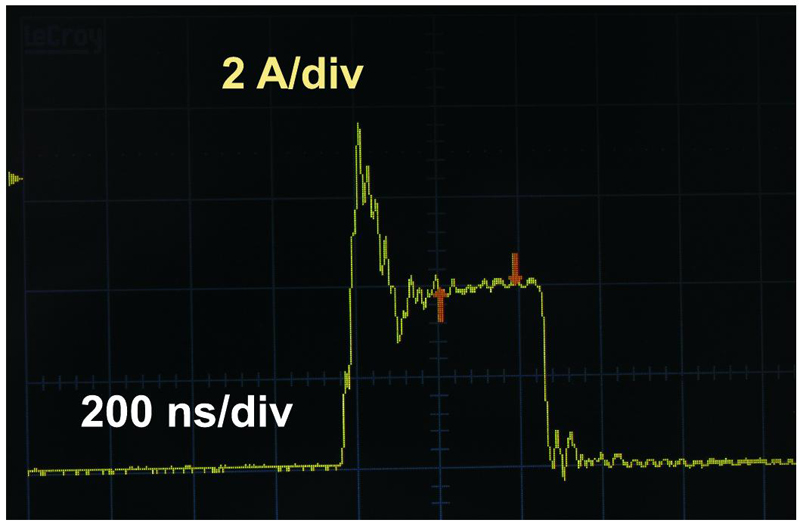
Figure 2 shows the primary current waveform under start-up conditions at high input line and with a short-circuited output. Refinements were made to the current-sensing gain and filtering to make sure the circuit was well protected under these conditions. Once this testing is done, you will find that you have a much higher confidence level in your circuit, and subsequent testing proceeds more smoothly.
The peak current observed in the power switch was 8 A under these conditions. A 20 MHz ringing was also seen on the waveform, and this was found to be a result of the new board layout which introduced some additional inductance in the primary traces. While not destructive, this ringing needs to be removed later with either a bypass capacitor, or changes to the layout. It was not seen in the earlier breadboard since a bypass capacitor was connected in a very short loop to the primary circuit.
Click image to enlarge
Figure 2: Primary Switch Current During Startup and Short-Circuit
Regulation Testing
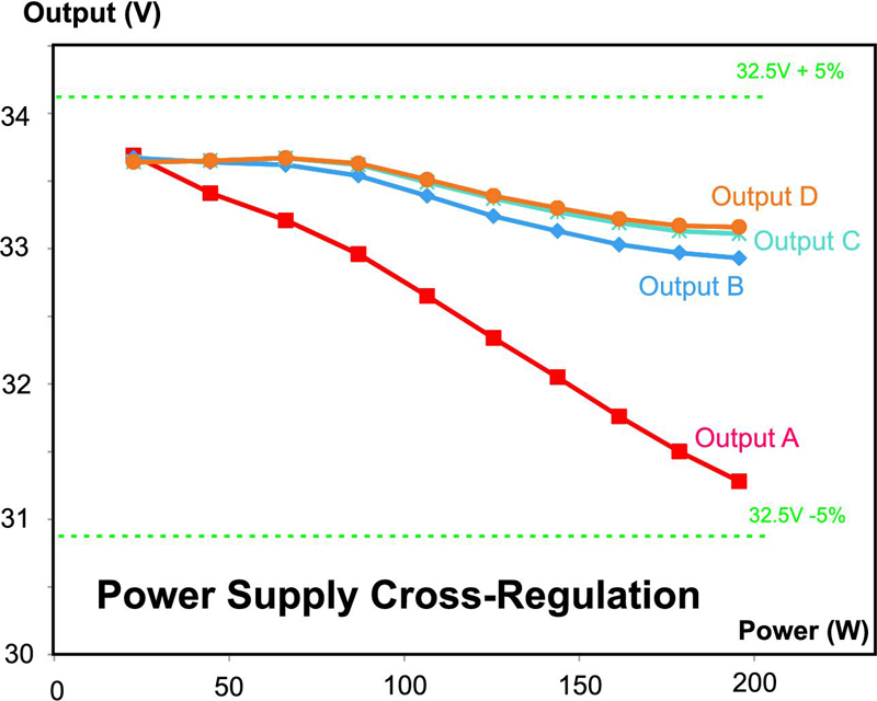
Figure 3 shows the regulation data for the five-output converter. The 12 V output was tightly regulated with a feedback loop, and Output A was loaded from 10% to full load. With this loading, the output dropped approximately 2.5 V as shown by the red curve. The other three outputs were minimally affected, dropping by only about 0.5 V. Output B, which was wound on the same layer as Output A showed the most variation.
Click image to enlarge
Figure 3: Output Regulation Data.
Most of the drop in output voltage was due to resistive losses which were considerably higher with the new design of the magnetics. Overall, it is expected that this power supply could maintain 5% regulation on each of the main outputs with loading over a ten-to-one range. This is a fairly typical result for cross-regulated converters that have been well designed. It is very important to maintain consistency in the magnetics design to ensure this quality of regulation.
Each of the other outputs was subsequently loaded over the same range, and very similar results were achieved for each. These results are not presented here since they essentially repeat the curves of Figure 3.
Voltage Measurements and Noise
When the cross-regulation results were first measured, results were very erratic. Fluke 79 meters were used on each of the outputs, and it was observed that these would not give accurate and repeatable measurements until high-frequency EMI issues were resolved. For example, holding onto the cables near the meters introduced more than 1 V variation in reading.
Engineers experienced with power supply design will be familiar with this problem. Sometimes solutions involve putting bypass capacitors at the input of the meters, but this is not always effective. The best solution is to provide proper EMI filters at the outputs of the power supply, as shown in the schematic of Figure 1. Once the common-mode filters were put in place, the measurements from the Fluke meter were accurate and repeatable.
Summary
Initial testing on the new revision of the power supply design and board layout properly established current limiting circuitry to ensure a rugged design. A nondestructive issue was detected with 20 MHz ringing in the primary current waveform, and a third iteration of the PCB will be required to fix this.
Initial testing of cross-regulation showed erratic measurements due to EMI noise pickup by the digital voltage meters. Once common-mode filters were placed on each of the outputs, the readings became reliable.
The five-output converter was found to have excellent cross-regulation, each output regulating within 5% over a ten-to-one load range.