Power Supply Management of GaN MMIC Power Amplifiers
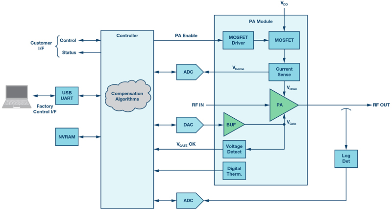
Figure 1. Typical GaN PA control system
Systems that incorporate highly integrated and highly sophisticated, high power radio frequency (RF) GaN power amplifiers (PAs), such as pulsed radar applications, are a constant challenge for today’s digital control and management systems to keep up with these ever-increasing levels of sophistication.These complex management systems require innovative compensation algorithms, built-in-test (BIT) features, local and remote communication interfaces, monitoring of critical system performance parameters and environmental conditions, and system fault protection. The increased complexity of these systems is driven by the demand for higher power from semiconductor-based RF systems.
These high power systems create a tremendous amount of heat, which has an impact on amplifier performance and mean times between failure (MTBF). The RF amplifier MMICs required for these systems ar eexpensive, high power devices. As a result, customers want to monitor the performance and temperature of the GaN PA-based systems in real-time. This allows for detection of impending problems in advance of damage so they can take the necessary actions to prevent it. With proper control electronics design, implementations can be extremely flexible and can be utilized with anyRFamplifierarchitecture.Thedigitalelectronicscanbetailoredtothe needs of the customer.The digital design can include built-in protectionlogic to disable the GaN RF amplifiers as damage thresholds are approached. These key features play a critical role in the need to optimize the RF performance over wide bandwidths and temperatures. They facilitate high levels of testability, maintainability, ease of system integration, and calibration—thus providing a technological differentiation.
Today’s semiconductor RF amplifiers continue to increase in complexity and output power. In order to optimize performance, manage power sequencing, provide fault detection, and provide amplifier system monitoring and protection, electronics can be implemented using reprogrammable field programmable gate arrays(FPGAs)and/or microcontrollers.There programmable solution provides the flexibility required for today’s development of advanced RF amplifier subsystems. The reprogrammability minimizes the risks of circuit board redesign and schedule delays due to design errors. These amplifier systems have similar, but different, requirements that are application dependent.The digital control electronics architecture is tailored to fit the application requirements and typically consists of:
- Digital controller
- Nonvolatile memory
- Analog-to-digital converter(ADC)
- Digital-to-analog converter(DAC)
- Digital input/output(I/O)
- DC power conditioning
- Communication interfaces
- Various analog sensors
Reuse of hardware and software is key to being able to develop design variants quickly and efficiently. These features reduce the time for factory test and calibration, and provide an important diagnostic tool that aids in the debug of system problems.
The majority of control systems for ADI RF amplifiers have utilized FPGAs. These devices are highly versatile and can include internal soft core or embedded processors. FPGAs can implement multiple parallel functions that can all operate simultaneously and independently.Therefore the FPGA has the ability to rapidly react to commands and critical circuit conditions to protect the RF electronics. Logic functions and algorithms are typically implemented in a hardware description language (HDL) such as Verilog or VHDL. Execution of logic functions are controlled by state-machine logic within the FPGA. A state-machine controls the sequence of operations performed based on the input and output conditions.
Optimization of amplifier performance: In order to optimize amplifier performance, the gate voltage must be set to achieve the amplifier specified power supply current in the data sheet. The gate voltage is adjusted with a DAC while monitoring the power amplifier’s power supply current using an ADC. These features provide the ability to rapidly calibrate the RF amplifier gate voltage without the need to probe or modify the RF electronics.
Enhanced power sequencing, power management, power supply monitoring:The FPGA design can be implemented to sequence voltage regulators and RF amplifiers to minimize power-upcurrent, and monitor and detect amplifie rand power supply faults.The FPGA can take protective action by shutting down system components based on detection of a fault condition, or report status via the control interface to a computer.The FPGA can manage overall system power dissipation by shutting down circuitry that is not actively being used (standbymode).
Temperature monitoring, thermal management: Temperature is a critical factor for RF performance in high power amplifier systems. Having the provision to monitor temperature allows the FPGA to implement algorithms that compensate amplifiers over temperature. Also, with temperature monitoring, the FPGA can be used to control cooling systems such as fan speed in order to minimize performance degradation.The logic can detect potentially damaging thermal conditions and take appropriate actions.
Digital and analog I/O: The FPGA can control RF switches, phase shifters,digital attenuators, and voltage variable attenuators (analog attenuators). Almost any analog sensor signal can be interfaced to the FPGA using ADCs. As long as the information of interest can be put into a digital form and connected to the FPGA, the information or signal of interest can be monitored and/or applied to an algorithm for processing.
Control, computer interfaces, graphicuserinterface (GUI):These are perhaps the most important aspects of the management system, as they provide easy access to all of the control,sensor, and diagnostic data available from the amplifier system. A GUI can be developed to form at all of the control and status information into an easy to use human interface. Software scripts may be developed to facilitate extremely high production test coverage, calibration, and failure analys is throughout system integration and final test.Test data can be written to computer files or read from computer files, and calibration data can be stored into NVRAM for use during run-time as variables to compensation algorithms. Beyond factory use, this powerful interface tool can be utilized in the field to monitor system health, determine system root cause failures, and provide easy field upgrades of control software. Variants of this interface can lend themselves easily to Internet of Things (IoT) applications, helping to bring intelligence to the edge.
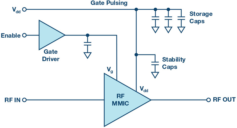
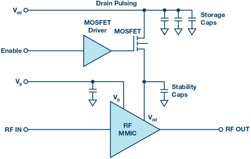
GaN RF power amplifiers are used in both continuous wave (CW) mode and pulsed mode applications. Pulsed operation is more challenging from a control standpoint, so it is the focus of this discussion. Pulsed RF may be utilized for communications,medical,and radar applications,to name a few. Pulsed operation has the benefit of reduced thermal dissipation facilitating less demanding cooling schemes and minimizes the systems external dc power requirements. However, increased pulsed repetition frequencies (PRFs) combined with lower duty cycles and faster settling time requirements continue to push the latest technology. Our approach to these demanding requirements has been to utilize digital control systems to pulse the RF MMICs. Field programmable gate arrays are typically used to enable/disable the RF MMICs using either gate or drain pulsing techniques depending on the system requirements. The FPGA’s control interface to the RF MMICs typically consists of circuitry to switch power to the MMIC’s drain, or some form of analog or digital-to-analog circuit that interfaces to the gate. Depending on switching speed and settling time requirements, capacitor banks may be required to store energy locally for most efficient dc biasing when pulsing the MMICs.
Figure 2 and Figure 3 illustrate generic, typical circuits that may beused for pulsed RF applications. The FPGA provides timing control of the pulsed signal, as well as provides synchronized status monitoring and protection for the RF MMICs. The FPGA can receive a single pulsed signal and distribute it to one, or many, RF MMIC devices, while maintaining a close timing relationship.
The benefit of gate pulsing in high power pulsed applications is that high dc switching is not required. However, gate pulsing may be complicated by the requirement that the gate voltage must be precise and well controlled to optimize the RF performance. MMIC characterization data is typically performed at a single static gate bias condition—where the MMIC performance is best. The MMICs are typically not characterizedfor pulsed operation. Some MMICs have exhibited instabilities when the gate voltages switch the MMIC between the pinch-off state and the on state. Drain pulsing may be more forgiving, and may require less MMICcharacterization data. Each pulsed application’s requirements must be carefully reviewed to determine the optimal pulsing methodology andcircuitry. Any MMIC pulsing application,either gate or drain pulsing, should be evaluated with the actual intended MMIC to be used in the design.
Click image to enlarge
Figure 2. Typical gate control scheme
Click image t enlarge
Figure 3. Typical drain switching scheme
Summary
To compete in this market, today’s control systems must be extremely flexible, reusable, and easily adaptable to various RF amplifier architectures that can be tailored to meet the needs of the customer. They can include built-in protection logic to disable the RF amplifiers as damage thresholds are approached and play a critical role in the need to optimize RF performance over wide bandwidths and operating temperatures. They facilitate high levels of testability, maintainability, ease of system integration, and calibration—thus providing a technological differentiation from competitors that impactfully innovates with today’s high power amplifier management systems.