Powering low-voltage devices from an intermediate-bus voltage
An overvoltage risk mitigation plan should be given careful consideration
Intermediate bus voltages from 24V to 28V (nominal) are commonplace in industrial, aerospace and defense systems, where series-connected batteries may be a backup power source and 12V bus architectures tend to be impractical due to distribution losses. The widening voltage gap between the system bus and the power inputs of digital processors present design challenges relating to power delivery, safety and solution size.
If a single-stage non-isolated step-down DC/DC converter is used, it must operate with extremely accurate PFM/PWM timing. Input surge events put further stress on the DC/DC converter, presenting another overvoltage risk to the load. Erroneous or counterfeit capacitors introduced in manufacturing may cause output voltage excursions exceeding the load’s ratings potentially causing the FPGA, ASIC or microprocessor to ignite. Depending on the extent of the damage, the root cause may be quite challenging to determine and the resulting high repair costs, downtime and harm to reputation extremely frustrating.
Therefore, an overvoltage risk mitigation plan should be given careful consideration to minimize cost and inconvenience to customers. Traditional overvoltage protection schemes involving a fuse are not suitable for protecting modern FPGAs, ASICs and microprocessors, particularly when the upstream voltage rail is 24V or 28V nominal. A new solution has been created, combining a 38V-rated, 10A DC/DC switching regulator with circuitry to defend against many faults, including output overvoltage. Power and protection for today’s most advanced digital logic devices are now available in one compact device.
Importance of accurate switcher timing
When a wide differential exists between the input voltage and the desired output voltage, switching DC/DC regulators are favored for their high efficiency. To achieve a small solution size, a non-isolated step-down switching converter is an obvious choice, operating at high enough frequency to shrink the size requirements of its power magnetics and filter capacitors. However, such a DC/DC switching converter must operate at narrow duty-cycles as low as 3%, which demands accurate PWM/PFM timing. Furthermore, tight voltage regulation is required by digital processors and fast transient response is needed to keep the voltage within safe limits. At higher input voltages, the margin for error in the on-time of the top side switch of the DC/DC regulator is reduced.
Bus voltage surges, which are often present in aerospace and defense applications, pose a danger not only to the DC/DC converter but to the load, as well. The DC/DC converter must be rated to regulate through the overvoltage surge with a fast control loop, so that sufficient line rejection is achieved. If the DC/DC converter fails to regulate or survive the bus surge, an overvoltage will be presented to the load. Overvoltage faults may also be introduced as the load’s bypass capacitors degrade with age and temperature, which results in looser transient load response over the course of the end product’s life.
If the capacitors degrade beyond the limits of the control loop’s design, the load can be exposed to overvoltage by two possible mechanisms. First, even if the control loop remains stable, heavy transient load-step events will demonstrate higher voltage excursions than were expected at the onset of design. Second, if the control loop becomes conditionally stable (or, worse yet, unstable), the output voltage can oscillate with peaks exceeding acceptable limits. Capacitors can also degrade unexpectedly or prematurely when an incorrect dielectric material is used, or when fake components enter the manufacturing flow.
Cheap counterfeits can cause costly headaches
Gray market or black market, the attractive cost of counterfeit components can prove to be too enticing for some to resist, even though they don’t meet the standards of the genuine article (e.g., they may be recycled, reclaimed from electronic waste, or built from inferior materials). A short-term savings becomes a huge expense when a counterfeit product fails. Counterfeit capacitors, for example, can fail in a number of ways. Counterfeit tantalum capacitors have been seen to suffer internal self-heating with a positive-feedback mechanism to the point of reaching thermal runaway. Counterfeit ceramic capacitors may contain compromised or inferior dielectric material, resulting in an accelerated loss of capacitance with age or at elevated operating temperatures. When capacitors fail catastrophically or degrade in value to induce control loop instability, the voltage waveforms can become much greater in amplitude than originally designed, endangering the load.
Risk mitigation planning
Any risk mitigation plan should consider how the system would respond to and recover from an overvoltage condition. Is the possibility of smoke or fire resulting from an overvoltage fault acceptable? Would efforts to determine root cause and implement corrective actions be hampered by damage resulting from an overvoltage fault? If a local operator were to power-cycle (reboot) a compromised system, would even greater harm to the system result further hindering recovery efforts? What is the process and time required to determine the cause of the fault and resume normal system operation?
Inadequacies of traditional protection circuits
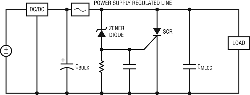
A traditional overvoltage protection scheme consists of a fuse, silicon controlled rectifier (SCR), and Zener diode. This circuit (Figure 1) protects the load in the following manner. If the input supply voltage exceeds the Zener breakdown voltage, the SCR activates, drawing sufficient current to blow open the upstream fuse. It is relatively simple and inexpensive, however drawbacks of this approach include accuracy of the Zener diode breakdown voltage, SCR gate trigger threshold variation, varying response time of the SCR and fuse and the level of effort required to recover from a fault (i.e. physically servicing the fuse and restarting the system).
If the voltage rail under consideration powers the digital core, the SCR’s protection capability is limited since the forward drop at high currents is comparable to or above the core voltage of the latest digital processors. Because of these drawbacks, the traditional overvoltage protection scheme is not suitable for high voltage to low voltage DC/DC conversion powering loads such as ASICs or FPGAs that could be valued in the hundreds if not thousands dollars.
While inexpensive, this circuit’s response time is insufficient to reliably protect the latest digital circuits particularly when the upstream supply rail is an intermediate voltage bus. Moreover, even the simplest recovery from an overvoltage fault is invasive and time consuming (see Figure 1).
Click image to enlarge
Figure 1. Traditional overvoltage protection circuit consisting of a fuse, SCR and Zener diode.
An innovation combining power & protection
A better solution would be to accurately detect an imminent overvoltage condition and respond by quickly disconnecting the input supply while discharging excess voltage at the load with a low impedance path, like the protection features included within the LTM4641 step-down µModule regulator. At the heart of the device is a 38V-rated, 10A step-down regulator with the inductor, control IC, power switches and compensation all contained in one surface mount package.
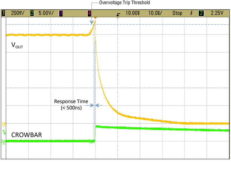
To add a level of protection for high value loads such as ASICs, FPGAs and microprocessors, an extensive level of monitoring and protection circuitry is included. The LTM4641 maintains a constant watch for input undervoltage, input overvoltage, overtemperature and output overvoltage and overcurrent conditions and acts appropriately to protect the load. To avoid false or premature execution of the protection features, each of these monitored parameters has built-in glitch immunity and user adjustable trigger thresholds with the exception of overcurrent protection, which is implemented reliably, cycle-by-cycle with current-mode control. In the case of an output overvoltage condition, the LTM4641 reacts within 500ns of fault detection (see Figure 2).
Click image to enlarge
Figure 2. The LTM4641 responds to an overvoltage condition within 500ns protecting the load from voltage stress. (VIN = 38V, VOUT = 1.0V, adjustable overvoltage trip threshold set at +11%)
Not only does the internal architecture of the LTM4641 allow it to respond nimbly and reliably, it can even automatically reset and rearm itself after fault conditions have subsided. A differential sense amplifier is employed to regulate the voltage at the load’s power terminals, minimizing errors stemming from common-mode noise and PCB trace voltage drops between the LTM4641 and the load. The DC voltage at the load is regulated to better than ±1.5% accuracy over line, load and temperature. This accurate output voltage measurement is also fed to the fast output overvoltage comparator, which triggers the LTM4641’s protection features.
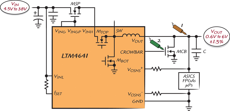
When an overvoltage condition is detected, the µModule regulator rapidly takes multiple courses of action, simultaneously. An external MOSFET (MSP in Figure 3) disconnects the input supply, removing the high voltage path from the regulator and the high-value load. Another external MOSFET (MCB in Figure 3) implements a low impedance crowbar function, quickly discharging the load’s bypass capacitors (C in Figure 3).
Click image to enlarge
Figure 3. LTM4641 output overvoltage protection plan. The two probe icons correspond with the waveforms in Figure 2.
The DC/DC step-down regulator within the LTM4641 enters a latched-off shutdown state and issues a fault signal indicated by the HYST pin which can be used by the system to initiate a well managed shutdown sequence and/or system reset. A dedicated voltage reference independent of the control loop’s reference voltage is used to detect fault conditions. This provides resilience against a single-point failure, should the control loop’s reference happen to fail.
The improvement in protection offered by the LTM4641 over the traditional fuse/SCR protection scheme is further bolstered by how the system recovers from a fault. In the traditional overvoltage protection scheme, a fuse is relied upon to separate the power supply from the high value load. Therefore, someone must physically be present to remove and replace the fuse in order for the system to resume normal operation after a fault has occurred. In contrast, the LTM4641 can resume normal operation quickly once the fault condition has cleared either by toggling a logic level control pin or by configuring the LTM4641 for autonomous restart after a user specified timeout period expires. No components need to be physically replaced, which is a critical requirement for systems with high uptime requirements and/or operating in remote locations. If fault conditions reappear after the LTM4641 resumes operation, the aforementioned protections immediately engage to again protect the load.
Input Surge Protection
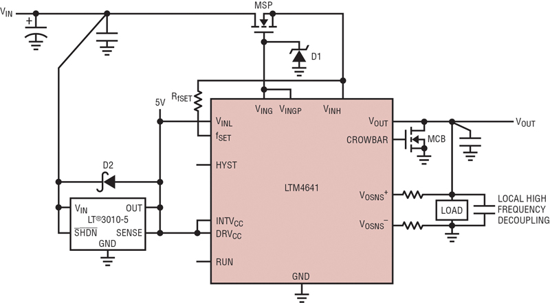
In some cases, output overvoltage protection alone is insufficient, and input overvoltage protection is desired. The LTM4641’s protection circuitry can monitor the input voltage and activate its protection features, should a user-configured voltage threshold be exceeded. If the anticipated maximum input voltage exceeds the 38V rating of the module, input surge protection can be extended up to 80V with the LTM4641 still fully operational by adding an external high voltage LDO, which keeps control and protection circuitry alive (see Figure 4).
Click image to enlarge
Figure 4. Input surge protection up to 80V, using the LTM4641 & external LDO
Conclusion
With market requirements for higher system performance and uptime coupled with the tremendous expense of the latest digital processors, engineers must consider risk mitigation strategies, particularly when a distributed power bus in range of 12V-28V or those with surges are involved. The latest and often very costly FPGAs, ASICs, and microprocessors have supply voltages with a maximum limit as low as 3% - 10% of the intermediate voltage rail, which makes them extremely susceptible to damage, potentially even igniting from an overvoltage fault. Such faults might be caused by timing errors in the switching regulator, an input voltage surge or improper components introduced during manufacture.
Acknowledgements:
Afshin Odabaee & Yan Liang, Linear Technology