Powering mobile devices with ICs just got easier
Much of the burden of a device’s reliability, run-time, and robustness falls on the power system
As with many other applications, low power precision components have enabled rapid growth of mobile devices. However, unlike many other applications, portable products targeted at industrial, medical and military applications typically have much higher standards for reliability, run time and robustness. Much of this burden falls on the power system and its components. A common feature of such products is that they must operate properly and switch seamlessly between a variety of power sources. As a result, great lengths must be taken to protect against and tolerate faults, maximize operating time when powered from batteries and ensure that operation is reliable whenever a valid power source is present.
Clearly, the power management integrated circuits (PMICs) required to address these needs must allow an application to receive power from multiple power sources; which could include: a wall adapter, a USB port, a car lighter adapter or even a Li-Ion battery. This can easily be done if the PMIC has integrated PowerPath control. This technique ensures that system power remains uninterrupted and tolerates hot plugging between external power and battery power. In some instances, a battery charger may also be included on the PMIC. If so, this battery-charging circuitry needs to ensure that the battery remains charged using excess power not needed by the application. Furthermore, on-chip protection circuitry is sometimes necessary to guard against external overvoltage faults exceeding 30V. Finally, low no-load quiescent current is essential to provide optimal power efficiency over a wide range of load and operating conditions. Features such as these are all critical to the success and utility of any products.
Industry Trends
While product form factors are decreasing, demand for their functionality and features are continuously increasing. Furthermore, the industry trend for sophisticated digital ICs such as microprocessors (µP) and microcontrollers (µC) or field programmable gate arrays (FPGAs) that power mobile products continue to lower their operating voltages while simultaneously increasing their amperage.
Microprocessors are among the most popular of these to design in, and there is a growing list of power efficient types from such suppliers as Freescale, Intel, NVIDIA, Samsung and others. They are designed to provide low power consumption and high performance processing for a wide range of portable, wireless and mobile device applications across multiple market segments.
The original intent of these processors was to enable OEMs to develop smaller and more cost-effective portable handheld devices with long battery life, while simultaneously offering enhanced computing performance to run feature-rich multimedia applications. Nevertheless, demand for this same combination of high power efficiency and processing performance has spread to non-portable applications.
A couple of examples include automotive infotainment systems and other embedded applications, both of which demand similar levels of power efficiency and processing horsepower. In all cases, a highly specialized, high performance power management IC is necessary to properly control and monitor the microprocessor’s power so that all of the performance benefits of these processors can be attained.
Many of today’s industrial and medical mobile devices require controlled and choreographed sequencing as power supplies are powered up and applied to various circuits. Allowing for system flexibility and a simple approach to sequencing not only makes the system design easier, but it also enhances system reliability and allows for a single PMIC to handle a broader range of the system than just a specific processor’s requirements.
Historically, many PMICs have not possessed the necessary power to handle these modern systems and microprocessors. Any solution to satisfy the Industrial or medical power management IC design constraints as already outlined must combine a high level of integration, including high-current switching regulators and LDOs, wide temperature range of operation, power sequencing and dynamic I2C control of key parameters with hard-to-do functional blocks.
Furthermore, a device with high switching frequency reduces the size of external components while ceramic capacitors reduce output ripple. This low ripple combines with accurate, fast response regulators to satisfy demanding voltage tolerances of 45nm type processors. Such power ICs must also be capable of meeting rigorous environmental constraints, such as radiated emission suppression, even if the input voltage is directly from the battery itself.
Design Challenges
Designers of today’s smart phones and tablets are faced with unprecedented challenges. Among these are the demands for high performance power management systems to accommodate growing system complexity and higher power budgets. These systems strive for an optimum balance among competing objectives including long battery runtime, compatibility with multiple power sources, high power density, small size and effective thermal management.
One common goal that all smart phones and tablets share is to reduce the amount of power they consume from their current levels. Power consumption in any system can be addressed in two ways, firstly by maximizing conversion efficiency across the entire range of load current, and secondly, by reducing the quiescent current drawn from the DC/DC converters in all modes of operation. Therefore, in order to have an active role in the reduction of system power consumption, power conversion and management ICs must be more efficient, with lower levels of power consumption under all operating conditions.
To address these specific requirements, Linear Technology incorporates its Burst Mode technology into many of its power management and conversion ICs. This technique minimizes the current needed by the IC itself during standby mode. In many cases, this standby quiescent current is less than 20μA.
Until recently, designers of Li-Ion battery-powered products have used two basic approaches to address the challenges of limited battery capacity within their small form factor. One choice is to architect the system using individual components, each optimized for a single function. This approach yields maximum flexibility in design, layout and thermal management while achieving the appropriate level of performance for each function. But this choice has the major disadvantage of being relatively costly and requiring substantial board space to address the growing list of functional requirements.
The other alternative is that designers may choose from a variety of highly integrated PMICs. These devices typically support a superset of the functionality needed for most applications, including unwieldy combinations of switching DC/DC controllers, monolithic switchers and numerous LDOs integrated with unrelated mixed signal functions like touch screen controllers, audio CODECs and more. As a result, they can be cumbersome to use and most require a substantial investment in firmware just to turn them on.
These products tend to favor integration over performance, and often complicate thermal management by concentrating heat in a single “hot spot” within the product. Ironically, these highly integrated solutions also require relatively more board space due to their large, high pin-count packages. Finally, they force board layout heroics in order to accommodate all the related external components (MOSFETs, inductors, diodes and assorted passive components) and associated trace routing needed to get from the PMIC to the various loads across the system.
However, a new approach is now available which is sandwiched between these two approaches of utilizing multiple power ICs or a highly complex PMICs, and that is a modestly integrated, yet powerful PMIC. Such and IC is the LTC3676/-1 recently released from Linear Technology.
The LTC3676/-1 are complete power management solutions for Freescale i.MX6 processors, ARM based processors and other advanced portable microprocessor systems. The LTC3676/-1 contain four synchronous step-down DC/DC converters at up to 2.5A each for core, memory, I/O and system on-chip (SoC) rails plus three 300mA linear regulators for low noise analog supplies. The LTC3676-1 configures a 1.5A buck regulator for source/sink and tracking operation to support DDR memory termination and also adds a VTTR reference output for DDR. These two pin features replace the LDO4 enable pin and feedback pins of the LTC3676. LDO4 is still programmable by I2C.
Supporting the multiple regulators is a highly configurable power sequencing capability, dynamic output voltage scaling, a pushbutton interface controller, plus regulator control via an I2C interface with extensive status and fault reporting via an interrupt output (see Figure 1). The LTC3676 supports i.MX6, PXA and OMAP processors with eight independent rails at appropriate power levels with dynamic control and sequencing. Other features include interface signals such as the VSTB pin that toggles between programmed run and standby output voltages on up to four rails simultaneously. The device is available in a low profile 40-pin 6mm x 6mm x 0.75mm exposed pad QFN package.
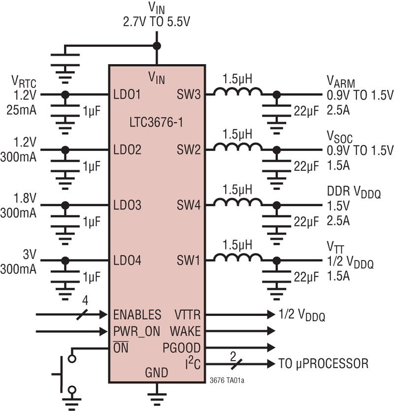
Click image to enlarge
Figure 1. LTC3676-1 Simplified Typical Application Diagram
The LTC3676 power management solution for application processors can solve the industrial and military system design challenges outlined above. The LTC3676IUJ is available in a high temperature (I-Grade) option with a junction temperature rating from -40°C to +125°C, easily satisfying the high temperature operating requirement. The IC includes a thermal warning flag and interrupt specifically for junction temperature monitoring and also includes a hard thermal shutdown for reliable protection of the hardware, should power dissipation be mismanaged, or in the event of a severe fault condition.
The LTC3676 PWM switching frequency is specifically trimmed to 2.25MHz with a guaranteed range of 1.7MHz to 2.7MHz. Its internal regulators can also be set to a forced continuous PWM operating mode to prevent operation in pulse skip or burst-mode even at light loads. This not only keeps the frequency fixed but also further reduces voltage ripple on the DC-DC output capacitors.
Conclusion
Designing a modern mobile device for the industrial, medical or military market segments is a challenging task due to the seemingly diametrical opposed requirements of high processing capability in an ever-shrinking form factor. However, thanks to suppliers like Linear Technology, systems designers now have the option to take a “middle ground” approach to resolving their power needs with a modestly integrated PMIC. This is a more practical approach when compared to using either individual ICs to build their system piece by piece or using highly integrated PMICs with all of their cumbersome functionality and firmware needs.
Either way, the choice is theirs to make.